

Philips TDF8712T, TDF8712, TDA8712T, TDA8712 Datasheet

INTEGRATED CIRCUITS
DATA SH EET
TDA8712; TDF8712
8-bit digital-to-analog converters
Product specification
Supersedes data of April 1993
File under Integrated Circuits, IC02
Philips Semiconductors
June 1994
Philips Semiconductors Product specification
8-bit digital-to-analog converters TDA8712; TDF8712
FEATURES
• 8-bit resolution
• Conversion rate up to 50 MHz
• TTL input levels
• Internal reference voltage generator
• Two complementary analog voltage outputs
• No deglitching circuit required
• Internal input register
• Low power dissipation
• Internal 75 Ω output load (connected to the analog
supply)
• Very few external components required
• Temperature range
– TDA8712: 0 to 70 °C
– TDF8712: −40 to +85 °C.
ORDERING INFORMATION
TYPE NUMBER
PINS PIN POSITION MATERIAL CODE
TDA8712 16 DIP plastic SOT38-1
TDF8712 16 DIP plastic SOT38-1
TDA8712T 16 SO16L plastic SOT162-1
TDF8712T 16 SO16L plastic SOT162-1
APPLICATIONS
• High-speed digital-to-analog conversion
• Digital TV including:
– field progressive scan
– line progressive scan
• Subscriber TV decoders
• Satellite TV decoders
• Digital VCRs
• Industrial and automotive.
GENERAL DESCRIPTION
The TDA8712 and TDF8712 are 8-bit digital-to-analog
converters (DACs) for video and other applications. They
convert the digital input signal into an analog voltage
output at a maximum conversion rate of 50 MHz. No
external reference voltage is required and all digital inputs
are TTL compatible.
PACKAGE
June 1994 2
Philips Semiconductors Product specification
8-bit digital-to-analog converters TDA8712; TDF8712
QUICK REFERENCE DATA
SYMBOL PARAMETER CONDITIONS MIN. TYP. MAX. UNIT
V
CCA
V
CCD
I
CCA
I
CCD
∆V
OUT(p-p)
ILE DC integral linear error −±0.3 ±0.5 LSB
DLE DC differential linearity error −±0.3 ±0.5 LSB
f
clk(max)
B −3 dB analog bandwidth f
P
tot
analog supply voltage
TDA8712 4.5 5.0 5.5 V
TDF8712 4.75 5.0 5.25 V
digital supply voltage
TDA8712 4.5 5.0 5.5 V
TDF8712 4.75 5.0 5.25 V
analog supply current note 1 20 26 32 mA
digital supply current note 1 16 23 30 mA
full-scale analog output voltage
differences between V
V
(peak-to-peak value)
OUT
OUT
and
ZL = 10 kΩ; note 2 −1.45 −1.60 −1.75 V
= 75 Ω; note 2 −0.72 0.80 −0.88 V
Z
L
maximum conversion rate 50 −−MHz
= 50 MHz; note 3 − 150 − MHz
clk
total power dissipation
TDA8712 160 250 340 mW
TDF8712 170 250 325 mW
Notes
1. D0 to D7 are connected to V
2. The analog output voltages (V
between V
and each of these outputs is typically 75 Ω.
CCA
and CLK is connected to DGND.
CCD
OUT
and V
) are negative with respect to V
OUT
(see Table 1). The output resistance
CCA
3. The −3 dB analog output bandwidth is determined by real time analysis of the output transient at a maximum input
code transition (code 0 to 255).
June 1994 3

Philips Semiconductors Product specification
8-bit digital-to-analog converters TDA8712; TDF8712
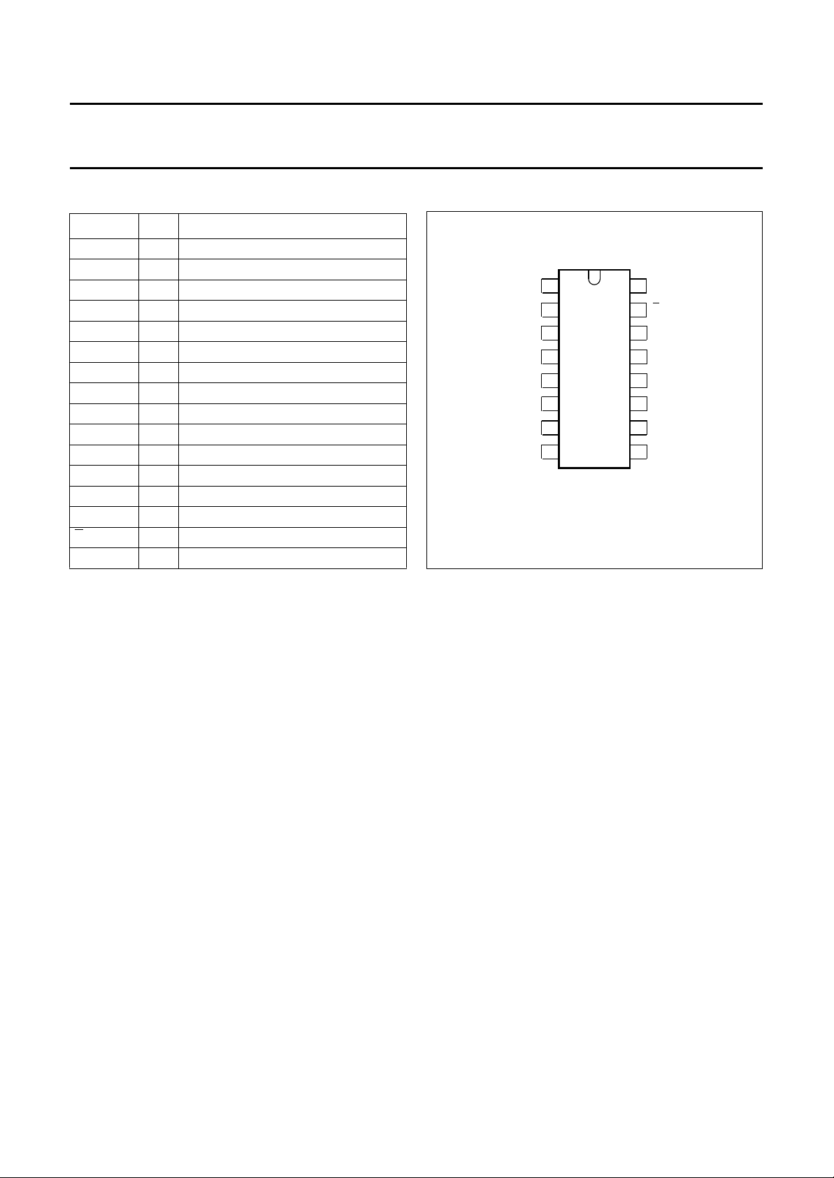
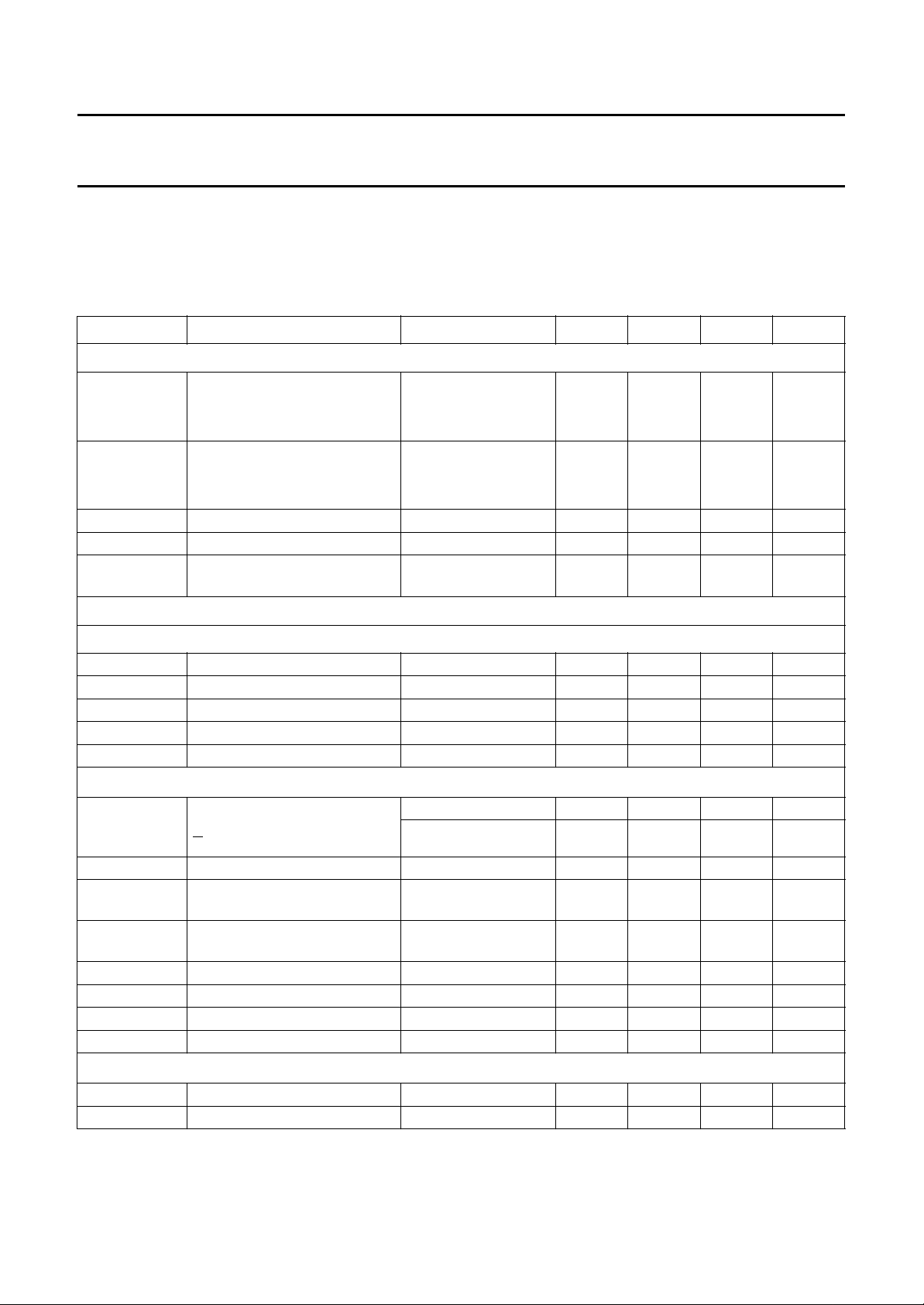
BLOCK DIAGRAM
handbook, full pagewidth
REF
100 nF
DGND
AGND
(LSB) D0
(MSB) D7
CLK
D1
D2
D3
D4
D5
D6
1
BAND-GAP
REFERENCE
6
2
5
CLOCK INPUT
INTERFACE
TDA8712
TDF8712
12
11
3
4
10
9
8
7
CURRENT
REFERENCE
LOOP
CURRENT
GENERATORS
CURRENT
SWITCHES
REGISTERS
DATA
INPUT
INTERFACE
16
V
CCA
75
75
Ω
Ω
15
V
V
V
OUT
OUT
CCD
14
Fig.1 Block diagram.
June 1994 4
MBC915 - 1
Philips Semiconductors Product specification
8-bit digital-to-analog converters TDA8712; TDF8712
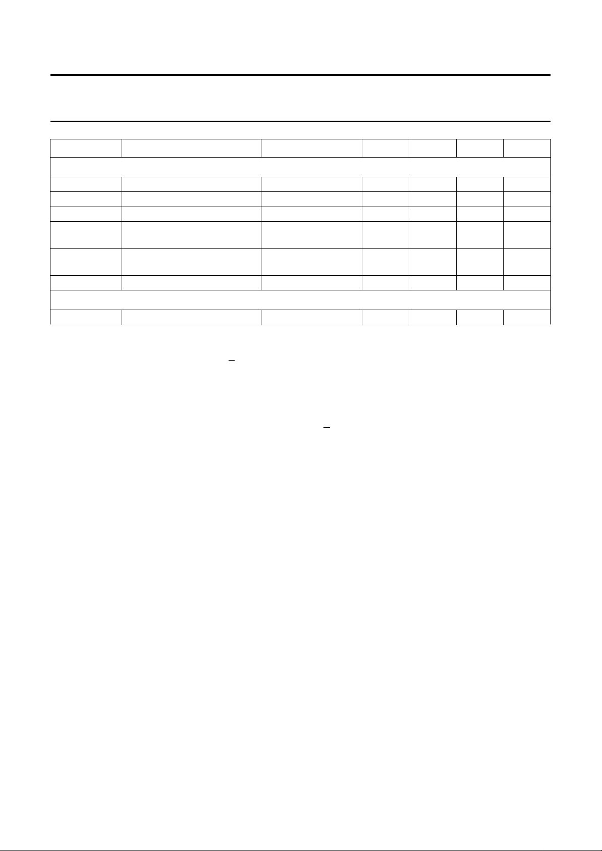
PINNING
SYMBOL PIN DESCRIPTION
REF 1 voltage reference (decoupling)
AGND 2 analog ground
D2 3 data input; bit 2
D3 4 data input; bit 3
CLK 5 clock input
DGND 6 digital ground
D7 7 data input; bit 7 (MSB)
D6 8 data input; bit 6
D5 9 data input; bit 5
D4 10 data input; bit 4
D1 11 data input; bit 1
D0 12 data input; bit 0 (LSB)
V
V
V
V
CCD
OUT
OUT
CCA
13 digital supply voltage (+5 V)
14 analog output voltage
15 complimentary analog output voltage
16 analog supply voltage (+5 V)
handbook, halfpage
1
REF
2
AGND
D2
3
D3
4
5
6
7
8
TDA8712
TDF8712
MBC901 - 1
CLK
DGND
D7
D6
Fig.2 Pin configuration.
V
16
CCA
V
15
OUT
V
14
OUT
V
13
CCD
D0
12
D1
11
D4
10
D5
9
June 1994 5
Philips Semiconductors Product specification
8-bit digital-to-analog converters TDA8712; TDF8712
LIMITING VALUES
In accordance with the Absolute Maximum Rating System (IEC134).
SYMBOL PARAMETER MIN. MAX. UNIT
V
V
∆V
∆V
V
I
tot
T
T
T
CCA
CCD
CC
GND
I
stg
amb
j
analog supply voltage −0.3 +7.0 V
digital supply voltage −0.3 +7.0 V
supply voltage differences between V
ground voltage differences between V
input voltage (pins 3 to 5 and 7 to 12) −0.3 V
total output current (I
OUT
+ I
; pins 14 and 15) −5 +26 mA
OUT
CCA
AGND
and V
and V
CCD
−0.5 +0.5 V
−0.1 +0.1 V
DGND
CCD
V
storage temperature −55 +150 °C
operating ambient temperature
TDA8712 0 +70 °C
TDF8712 −40 +85 °C
junction temperature − +150 °C
HANDLING
Inputs and outputs are protected against electrostatic discharges in normal handling. However, to be totally safe, it is
desirable to take normal precautions appropriate to handling integrated circuits.
THERMAL CHARACTERISTICS
SYMBOL PARAMETER VALUE UNIT
R
th j-a
thermal resistance from junction to ambient in free air
SOT38-1 70 K/W
SOT162-1 90 K/W
June 1994 6
Philips Semiconductors Product specification
8-bit digital-to-analog converters TDA8712; TDF8712
CHARACTERISTICS
V
= V16 to V2 = 4.5 to 5.5 V (TDA8712) = 4.75 to 5.25 V (TDF8712); V
CCA
4.75 to 5.25 V (TDF8712); V
AGND via a 100 nF capacitor; T
V
CCA=VCCD
= 5 V and T
to V
CCA
amb
= 25 °C; unless otherwise specified.
amb
= −0.5 to +0.5 V (TDA8712) = −0.25 to +0.25 V (TDF8712); REF decoupled to
CCD
= −40 to +85 °C; AGND and DGND shorted together; typical readings taken at
SYMBOL PARAMETER CONDITIONS MIN. TYP. MAX. UNIT
Supply
V
CCA
analog supply voltage
TDA8712 4.5 5.0 5.5 V
TDF8712 4.75 5.0 5.25 V
V
CCD
digital supply voltage
TDA8712 4.5 5.0 5.5 V
TDF8712 4.75 5.0 5.25 V
I
CCA
I
CCD
∆V
GND
analog supply current note 1 20 26 32 mA
digital supply current note 1 16 23 30 mA
ground voltage differences
between V
AGND
and V
DGND
Inputs
= V13to V6 = 4.5 to 5.5 V (TDA8712) =
CCD
−0.1 − +0.1 V
IGITAL INPUTS (D7 TO D0) AND CLOCK INPUT CLK
D
V
IL
V
IH
I
IL
I
IH
f
clk(max)
Outputs (referenced to V
∆V
OUT(p-p)
V
os
TC
VOUT
LOW level input voltage 0 − 0.8 V
HIGH level input voltage 2.0 − V
CCD
V
LOW level input current VI= 0.4 V −−0.3 −0.4 mA
HIGH level input current VI= 2.7 V − 0.01 20 µA
maximum clock frequency 50 −−MHz
)
CCA
full-scale analog output voltage
differences between V
V
(peak-to-peak value)
OUT
OUT
ZL = 10 kΩ; note 2 −1.45 −1.60 −1.75 V
and
= 75 Ω; note 2 −0.72 0.80 −0.88 V
Z
L
analog offset output voltage code = 0 −−3−25 mV
full-scale analog output voltage
−−200 µV/K
temperature coefficient
TC
Vos
analog offset output voltage
−−20 µV/K
temperature coefficient
B −3 dB analog bandwidth f
G
diff
ϕ
diff
Z
o
Transfer function (f
differential gain − 0.6 − %
differential phase − 1 − deg
output impedance − 75 −Ω
= 50 MHz)
clk
= 50 MHz; note 3 − 150 − MHz
clk
ILE DC integral linear error −±0.3 ±0.5 LSB
DLE DC differential linearity error −±0.3 ±0.5 LSB
June 1994 7
Philips Semiconductors Product specification
8-bit digital-to-analog converters TDA8712; TDF8712
SYMBOL PARAMETER CONDITIONS MIN. TYP. MAX. UNIT
Switching characteristics (f
t
SU;DAT
t
HD;DAT
t
PD
t
S1
data set-up time −0.3 −−ns
data hold time 2.0 −−ns
propagation delay time −−1.0 ns
settling time 1 10% to 90% full-scale
= 50 MHz; notes 4 and 5; see Figs 3, 4 and 5)
clk
− 1.1 1.5 ns
change to ±1 LSB
t
S2
settling time 2 10% to 90% full-scale
− 6.5 8.0 ns
change to ±1 LSB
t
d
Output transients (glitches; f
E
g
input to 50% output delay time − 3.0 5.0 ns
= 50 MHz; note 6; see Fig.6)
clk
glitch energy from code transition 127 to 128 −−30 LSB⋅ns
Notes
1. D0 to D7 are connected to V
2. The analog output voltages (V
between V
and each of these outputs is typically 75 Ω.
CCA
and CLK is connected to DGND.
CCD
OUT
and V
) are negative with respect to V
OUT
(see Table 1). The output resistance
CCA
3. The −3 dB analog output bandwidth is determined by real time analysis of the output transient at a maximum input
code transition (code 0 to 255).
4. The worst case characteristics are obtained at the transition from input code 0 to 255 and if an external load
impedance greater than 75 Ω is connected between V
measured with an active probe between V
and AGND. No further load impedance between V
OUT
OUT
or V
OUT
and V
. The specified values have been
CCA
and AGND has
OUT
been applied. All input data is latched at the rising edge of the clock. The output voltage remains stable (independent
of input data variations) during the HIGH level of the clock (CLK = HIGH). During a LOW-to-HIGH transition of the
clock (CLK = LOW), the DAC operates in the transparent mode (input data will be directly transferred to their
corresponding analog output voltages; see Fig.5.
5. The data set-up time (t
) is the minimum period preceding the rising edge of the clock that the input data must
SU;DAT
be stable in order to be correctly registered. A negative set-up time indicates that the data may be initiated after the
rising edge of the clock and still be recognized. The data hold time (t
) is the minimum period following the rising
HD;DAT
edge of the clock that the input data must be stable in order to be correctly registered. A negative hold time indicates
that the data may be released prior to the rising edge of the clock and still be recognized.
6. The definition of glitch energy and the measurement set-up are shown in Fig.6. The glitch energy is measured at the
input transition between code 127 and 128 and on the falling edge of the clock.
June 1994 8
 Loading...