

Philips tdf8704 DATASHEETS

INTEGRATED CIRCUITS
DATA SH EET
TDF8704
8-bit high-speed analog-to-digital
converter
Product specification
Supersedes data of April 1993
File under Integrated Circuits, IC02
Philips Semiconductors
June 1994
Philips Semiconductors Product specification
8-bit high-speed analog-to-digital converter TDF8704
FEATURES
• 8-bit resolution
• Sampling rate up to 50 MHz
• Extended temperature range (−40 to +85 °C)
• High signal-to-noise ratio over a large analog input
frequency range (7.4 effective bits at 4.43 MHz full-scale
input and at f
= 50 MHz)
clk
• Binary 3-state TTL outputs
• Overflow/underflow 3-state TTL output
• TTL compatible digital inputs
• Low-level AC clock input signal allowed
• Stable internal reference voltage regulator included
• Power dissipation only 380 mW (typical)
• Low analog input capacitance, no buffer amplifier
required
• No sample-and-hold circuit required.
QUICK REFERENCE DATA
APPLICATIONS
• General purpose high-speed analog-to-digital
conversion for extended temperature applications
• Automotive
• RF, satellite and GPS (Global Positioning System)
• Medical
• General industrial
• Digital video (VCR, TV and satellite).
GENERAL DESCRIPTION
The TDF8704T is an 8-bit high-speed analog-to-digital
converter (ADC) for general industrial applications. It
converts the analog input signal into 8-bit binary-coded
digital words at a maximum sampling rate of 50 MHz. All
digital inputs and outputs are TTL compatible, although a
low-level AC clock input signal is allowed.
SYMBOL PARAMETER CONDITIONS MIN. TYP. MAX. UNIT
V
V
V
I
CCA
I
CCD
I
CCO
CCA
CCD
CCO
analog supply voltage 4.75 5.0 5.25 V
digital supply voltage 4.75 5.0 5.25 V
output stages supply voltage 4.75 5.0 5.25 V
analog supply current − 37 46 mA
digital supply current − 23 35 mA
output stages supply current − 16 21 mA
ILE DC integral linear error −±0.4 ±1 LSB
DLE DC differential linearity error −±0.2 ±0.5 LSB
AILE AC integral linearity error note 1 −−±2 LSB
f
clk(max)
P
tot
maximum clock frequency 50 −−MHz
total power dissipation − 380 535 mW
Note
1. Full-scale sine wave (f
= 4.43 MHz; f
i
= 50 MHz).
clk
ORDERING INFORMATION
TYPE NUMBER
PACKAGE
PINS PIN POSITION MATERIAL CODE
SAMPLING
FREQUENCY
TDF8704T/2 24 SO24L plastic SOT137-1 20 MHz
TDF8704T/4 24 SO24L plastic SOT137-1 40 MHz
TDF8704T/5 24 SO24L plastic SOT137-1 50 MHz
June 1994 2
Philips Semiconductors Product specification
8-bit high-speed analog-to-digital converter TDF8704
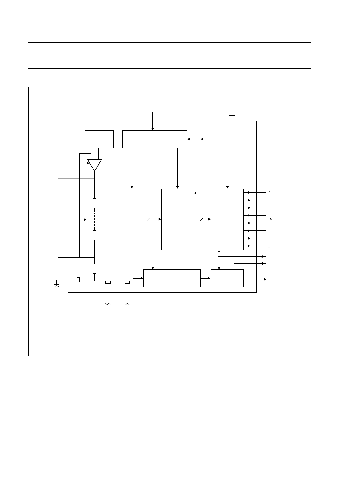
BLOCK DIAGRAM
handbook, full pagewidth
V
RT
V
RB
OGND
V
analog
voltage input
output ground
V
CCA
7
STABILIZER
5DEC
9
I
8
4
20
TDF8704
ANALOG - TO - DIGITAL
CONVERTER
6
AGND
17
DGND
CLK
16
CLOCK DRIVER
LATCHES
OVERFLOW / UNDERFLOW
LATCH
V
CCD
18
TTL OUTPUTS
TTL OUTPUT
CE
22
12
13
14
15
23
24 D2
19
21
11
MSA685
D7
D6
D5
D4
D3
1
D1
2
D0
MSB
data outputs
LSB
V
CCO1
V
CCO2
overflow / underflow
output
analog ground digital ground
Fig.1 Block diagram.
June 1994 3
Philips Semiconductors Product specification
8-bit high-speed analog-to-digital converter TDF8704
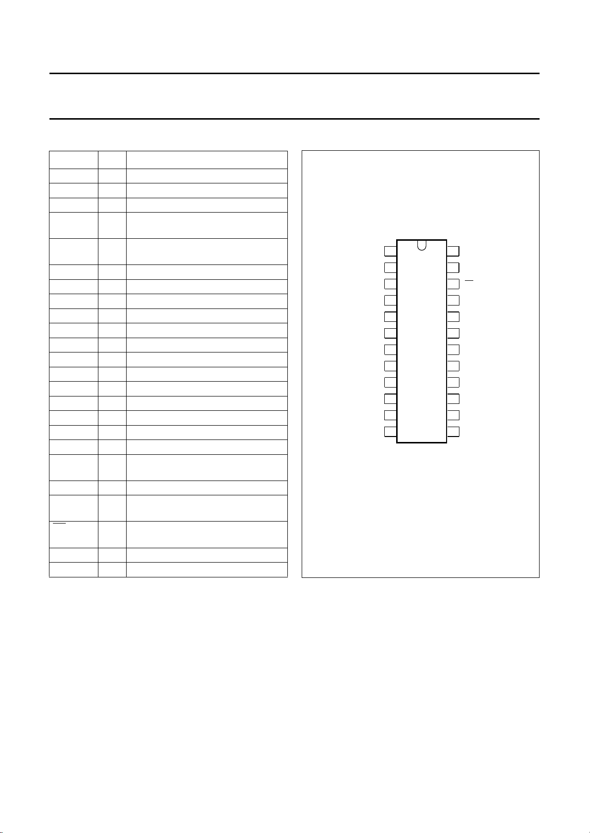
PINNING
SYMBOL PIN DESCRIPTION
D1 1 data output; bit 1
D0 2 data output; bit 0 (LSB)
n.c. 3 not connected
V
RB
DEC 5 decoupling input (internal
AGND 6 analog ground
V
CCA
V
I
V
RT
n.c. 10 not connected
O/UF 11 overflow/underflow data output
D7 12 data output; bit 7 (MSB)
D6 13 data output; bit 6
D5 14 data output; bit 5
D4 15 data output; bit 4
CLK 16 clock input
DGND 17 digital ground
V
CCD
V
CCO1
OGND 20 output ground
V
CCO2
CE 22 chip enable input (TTL level input,
D3 23 data output; bit 3
D2 24 data output; bit 2
4 reference voltage BOTTOM
(decoupling)
stabilization loop decoupling)
7 analog supply voltage (+5 V)
8 analog input voltage
9 reference voltage TOP (decoupling)
18 digital supply voltage (+5 V)
19 supply voltage for output stages 1
(+5 V)
21 supply voltage for output stages 2
(+5 V)
active LOW)
handbook, halfpage
1
D1
2
D0
3
n.c.
V
RB
4
5
DEC
AGND
6
V
CCA
V
O/UF
V
RT
n.c.
D7
TDF8704
7
8
I
9
10
11
12
MSA686
Fig.2 Pin configuration.
24
D2
D3
23
22
CE
V
21
CCO2
OGND
20
V
CCO1
19
V
CCD
18
17
DGND
CLK
16
D4
15
D5
14
D6
13
June 1994 4
Philips Semiconductors Product specification
8-bit high-speed analog-to-digital converter TDF8704
LIMITING VALUES
In accordance with the Absolute Maximum Rating System (IEC134).
SYMBOL PARAMETER CONDITIONS MIN. MAX. UNIT
V
CCA
V
CCD
V
CCO
∆V
∆V
∆V
V
I
V
clk(p-p)
I
O
T
stg
T
amb
T
j
CC
CC
CC
analog supply voltage −0.3 +7.0 V
digital supply voltage −0.3 +7.0 V
output stages supply voltage −0.3 +7.0 V
supply voltage differences between V
supply voltage differences between V
supply voltage differences between V
CCA
CCO
CCA
and V
and V
and V
CCD
CCD
CCO
−1.0 +1.0 V
−1.0 +1.0 V
−1.0 +1.0 V
input voltage referenced to AGND −0.3 +7.0 V
AC input voltage for switching (peak-to-peak value) referenced to DGND − V
CCD
V
output current − 10 mA
storage temperature −55 +150 °C
operating ambient temperature −40 +85 °C
junction temperature − +150 °C
HANDLING
Inputs and outputs are protected against electrostatic discharges in normal handling. However, to be totally safe, it is
desirable to take normal precautions appropriate to handling integrated circuits.
THERMAL CHARACTERISTICS
SYMBOL PARAMETER VALUE UNIT
R
th j-a
thermal resistance from junction to ambient in free air 75 K/W
June 1994 5
Philips Semiconductors Product specification
8-bit high-speed analog-to-digital converter TDF8704
CHARACTERISTICS (see Tables 1 and 2)
V
= V7 to V6 = 4.75 to 5.25 V; V
CCA
and DGND shorted together; V
V
CCA
to V
= −0.25 to +0.25 V; T
CCD
CCA
unless otherwise specified.
SYMBOL PARAMETER CONDITIONS MIN. TYP. MAX. UNIT
Supply
V
V
V
I
CCA
I
CCD
I
CCO
CCA
CCD
CCO
analog supply voltage 4.75 5.0 5.25 V
digital supply voltage 4.75 5.0 5.25 V
output stages supply voltage 4.75 5.0 5.25 V
analog supply current − 37 46 mA
digital supply current − 23 35 mA
output stages supply current all outputs LOW − 16 21 mA
Inputs
= V18to V17 = 4.75 to 5.25 V; V
CCD
to V
amb
= −0.25 to +0.25 V; V
CCD
= −40 to +85 °C; typical readings taken at V
CCO
CCO
to V
= V19and V21to V20 = 4.75 to 5.25 V; AGND
= −0.25 to +0.25 V;
CCD
CCA=VCCD
= 5 V and T
amb
=25°C;
LOCK INPUT CLK (REFERENCED TO DGND)
C
V
IL
V
IH
I
IL
I
IH
Z
I
C
I
LOW level input voltage 0 − 0.8 V
HIGH level input voltage 2.0 − V
LOW level input current V
HIGH level input current V
input impedance f
input capacitance f
= 0.4 V −400 −−µA
clk
= 2.7 V −−100 µA
clk
V
clk=VCCD
= 50 MHz − 2 − kΩ
clk
= 50 MHz − 4.5 − pF
clk
−−300 µA
VI(ANALOG INPUT VOLTAGE REFERENCED TO AGDN; SEE FIGS 3 AND 4 AND TABLE 1)
V
V
V
V
V
V
V
I(B)
I(0)
os(B)
I(T)
I(255)
os(T)
I(p-p)
input voltage (BOTTOM) 1.21 1.25 1.29 V
input voltage output code = 0 1.42 1.48 1.51 V
offset voltage (BOTTOM) V
I(0)
to V
I(B)
210 225 240 V
input voltage (TOP) 3.37 3.46 3.58 V
input voltage output code = 255 3.14 3.22 3.30 V
offset voltage (TOP) V
input voltage amplitude
I(T)
to V
I(255)
225 240 255 V
1.69 1.74 1.79 V
(peak-to-peak value)
I
L
I
IL
I
IH
Z
I
C
I
load current on VRT and V
RB
LOW level input current VI = 1.25 V − 0 −µA
HIGH level input current VI = 3.46 V 40 150 400 µA
input impedance fi = 4.43 MHz − 10 − kΩ
input capacitance fi = 4.43 MHz − 14 − pF
−300 − +300 µA
CCD
V
June 1994 6
 Loading...