

Philips tdf5242t DATASHEETS

INTEGRATED CIRCUITS
DATA SH EET
TDF5242T
Brushless DC motor drive circuit
Preliminary specification
Supersedes data of 1997 Apr 23
File under Integrated Circuits, IC11
1997 Sep 12

Philips Semiconductors Preliminary specification
Brushless DC motor drive circuit TDF5242T
FEATURES
• Full-wave commutation without position sensors
• Built-in start-up circuitry
• Six outputs that can drive three external transistor pairs:
APPLICATIONS
• High-power applications, for instance:
– high-end hard disk drives
– automotive applications.
– output current 0.2 A (typ.)
– low saturation voltage
– built-in current limiter
• Thermal protection
• Tacho output without extra sensor
• Transconductance amplifier for an external control
transistor
• Brake control input
• Direction control input.
GENERAL DESCRIPTION
The TDF5242T is a bipolar integrated circuit for driving
3-phase brushless DC motors in full-wave mode.
The device functions sensorless, thus saving 3 hall-effect
sensors, using the back-EMF (Electro Motive Force)
sensing technique to sense the rotor position. It includes
6 pre-drivers able to control external FETs (Field Effect
Transistors) or bipolar transistors. It offers brake and
direction control. It is ideally suited for high-power
applications such as high-end hard disk drives and
automotive applications.
QUICK REFERENCE DATA
Measured over full voltage and temperature range.
SYMBOL PARAMETER CONDITIONS MIN. TYP. MAX. UNIT
V
P
V
VMOT
supply voltage note 1 4 − 18 V
input voltage to the output
3 − 18 V
driver stages
V
O
I
LIM
driver output voltage IO= 100 mA; lower transistor −−0.35 V
I
= 100 mA; upper transistor 1.05 −−V
O
current limiting V
= 14.5 V; RO=47Ω 150 200 250 mA
VMOT
Note
1. An unstabilized supply can be used.
ORDERING INFORMATION
TYPE
NUMBER
NUMBER DESCRIPTION VERSION
PACKAGE
TDF5242T SO28 plastic small outline package; 28 leads; body width 7.5 mm SOT136-1
1997 Sep 12 2
Philips Semiconductors Preliminary specification
Brushless DC motor drive circuit TDF5242T
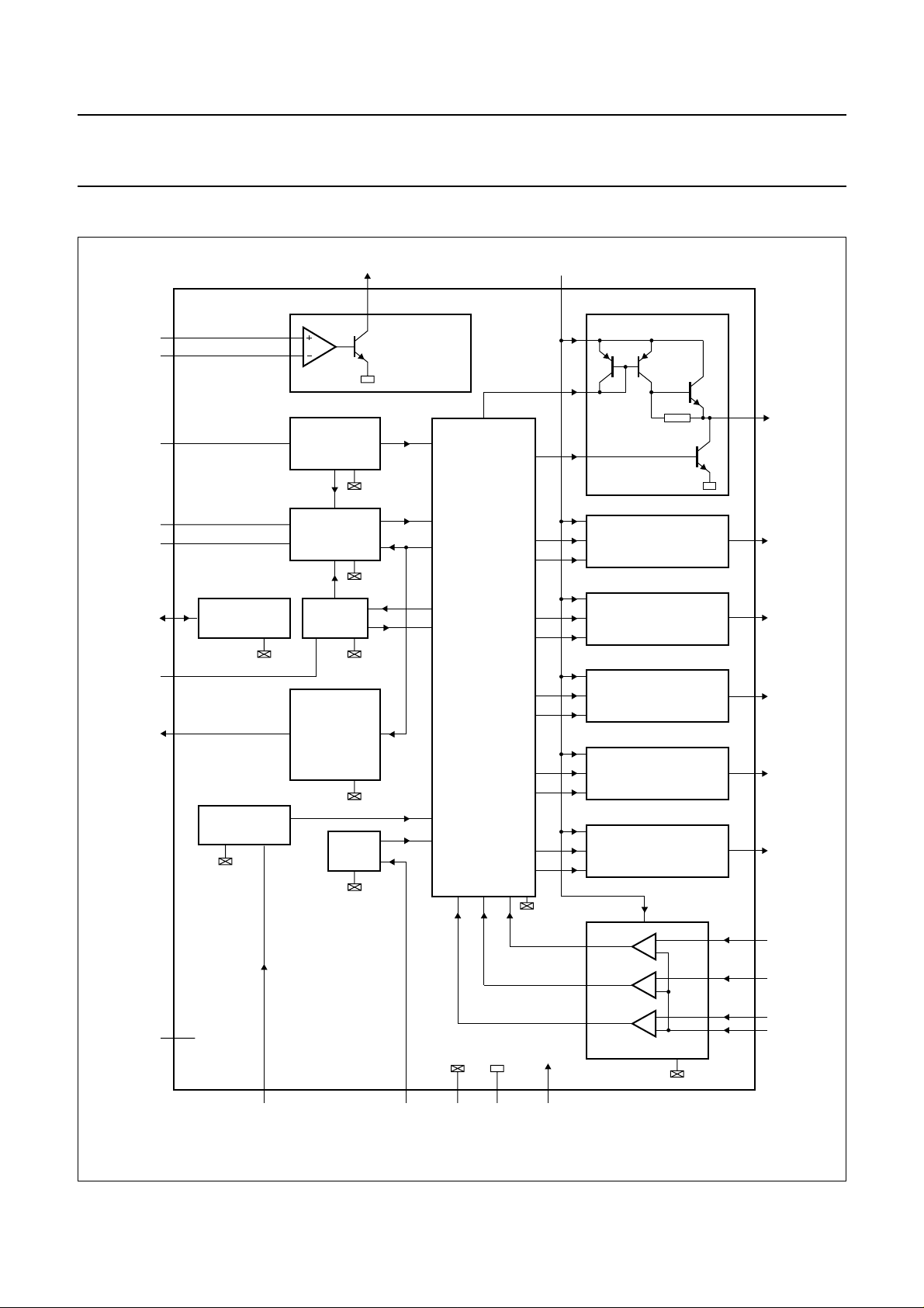
BLOCK DIAGRAM
handbook, full pagewidth
+AMP IN
−AMP IN
CAP-ST
CAP-DC
CAP-CD
TEST
CAP-TI
FG
19
20
16
15
14
8
18
10
THERMAL
PROTECTION
AMP OUT VMOT
START-UP
OSCILLATOR
ADAPTIVE
COMMUTATION
DELAY
TIMING
ROTATION
SPEED
AND
DETECTOR
OUTPUT
STAGE
21 6
TRANS-
CONDUCTANCE
AMPLIFIER
COMMUTATION
LOGIC
OUTPUT DRIVER STAGE
OUTPUT DRIVER
STAGE
OUTPUT DRIVER
STAGE
OUTPUT DRIVER
STAGE
OUTPUT DRIVER
STAGE
27
OUT-NA
28
OUT-PA
1
OUT-NB
2
OUT-PB
4
OUT-PC
DIRECTION
LOGIC
BRAKE
LOGIC
TDF5242T
12, 17, 25
n.c.
7
DIR BRAKE GND2 GND1 V
9113
Fig.1 Block diagram.
1997 Sep 12 3
EMF COMPARATORS
13
P
OUTPUT DRIVER
STAGE
22
23
24
26
MGG988
5
OUT-NC
COMP-A
COMP-B
COMP-C
MOT0
Philips Semiconductors Preliminary specification
Brushless DC motor drive circuit TDF5242T
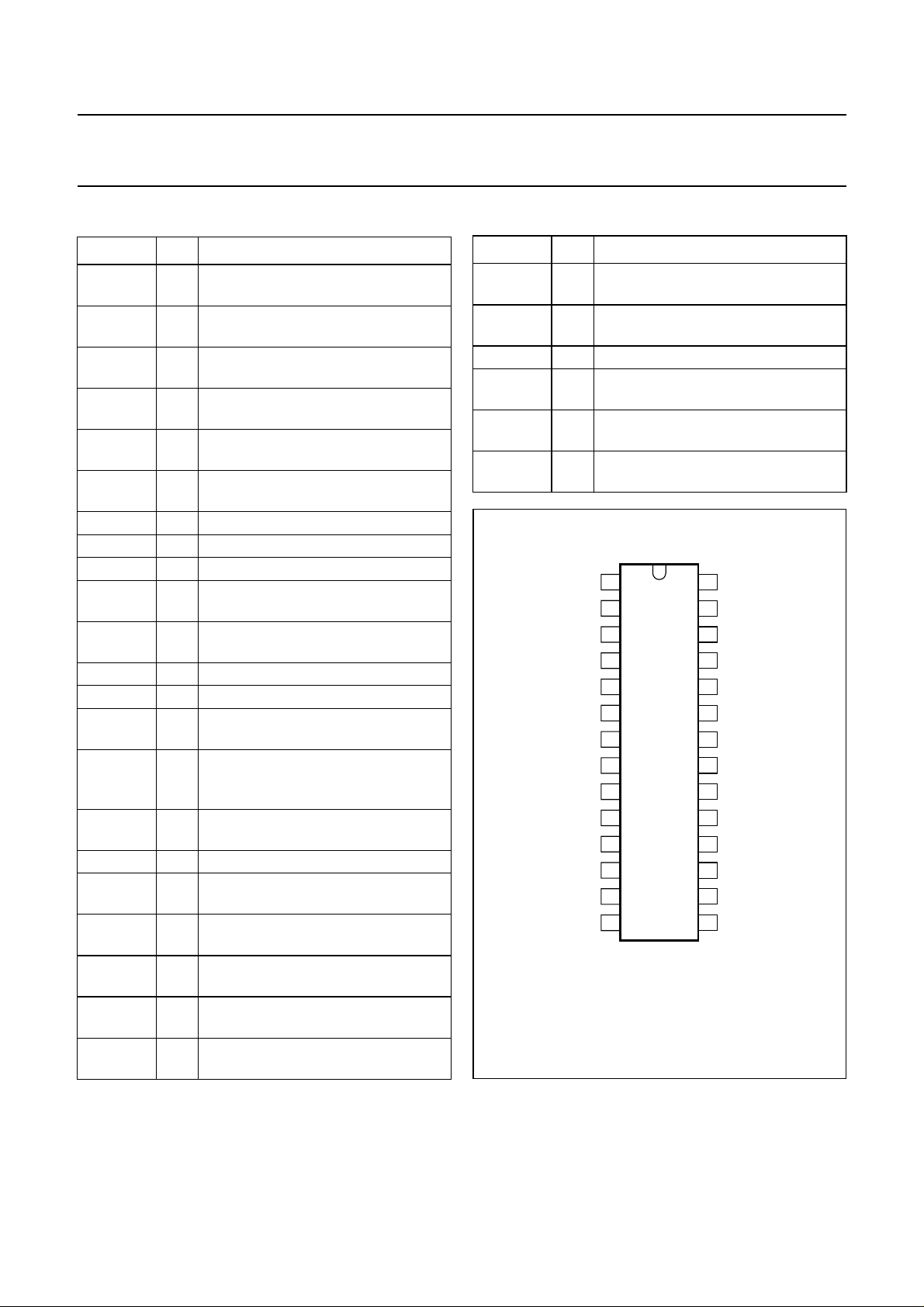
PINNING
SYMBOL PIN DESCRIPTION
OUT-NB 1 driver output B for driving the
n-channel power FET or power NPN
OUT-PB 2 driver output B for driving the
p-channel power FET or power PNP
GND1 3 ground (0 V) motor supply return for
output stages
OUT-PC 4 driver output C for driving the
p-channel power FET or power PNP
OUT-NC 5 driver output C for driving the
n-channel power FET or power NPN
VMOT 6 input voltage for the output driver
stages
DIR 7 direction input command
TEST 8 test input/output
BRAKE 9 brake input
FG 10 frequency generator: output of the
rotation speed detector stage
GND2 11 ground supply return for control
circuits
n.c. 12 not connected
V
P
13 supply voltage
CAP-CD 14 external capacitor connection for
adaptive communication delay timing
CAP-DC 15 external capacitor connection for
adaptive communication delay
timing copy
CAP-ST 16 external capacitor connection for
start-up oscillator
n.c. 17 not connected
CAP-TI 18 external capacitor connection for
timing
+AMP IN 19 non-inverting input of the
transconductance amplifier
−AMP IN 20 inverting input of the
transconductance amplifier
AMP OUT 21 transconductance amplifier output
(open collector)
COMP-A 22 comparator input corresponding to
output A
SYMBOL PIN DESCRIPTION
COMP-B 23 comparator input corresponding to
output B
COMP-C 24 comparator input corresponding to
output C
n.c. 25 not connected
MOT0 26 input from the star point of the motor
coils
OUT-NA 27 driver output A for driving the
n-channel power FET or power NPN
OUT-PA 28 driver output A for driving the
p-channel power FET or power PNP
handbook, halfpage
OUT-NB
OUT-PB
GND1
OUT-PC
OUT-NC
VMOT
DIR
TEST
BRAKE
FG
GND2
n.c.
V
CAP-CD
P
1
2
3
4
5
6
7
TDA5242T
8
9
10
11
12
13
MGG987
28
27
26
25
24
23
22
21
20
19
18
17
16
1514
OUT-PA
OUT-NA
MOT0
n.c.
COMP-C
COMP-B
COMP-A
AMP OUT
−AMP IN
+AMP IN
CAP-TI
n.c.
CAP-ST
CAP-DC
Fig.2 Pin configuration.
1997 Sep 12 4

Philips Semiconductors Preliminary specification
Brushless DC motor drive circuit TDF5242T
FUNCTIONAL DESCRIPTION
Introduction
Full-wave driving of a three phase motor requires three
push-pull output stages. In each of the six possible states
two outputs are active, one sourcing (H) and one sinking
(L). The third output presents a high impedance (Z) to the
motor, which enables measurement of the motor
back-EMF (Electro Motive Force) in the corresponding
motor coil by the EMF comparator at each output.
The commutation logic is responsible for control of the
output transistors and selection of the correct EMF
comparator. In Table 1, the six possible states of the
externally connected output transistors have been
depicted and the corresponding output levels on the NA,
PA, NB, PB, NC and PC outputs of the TDF5242T.
The zero-crossing in the motor EMF (detected by the
comparator selected by the commutation logic) is used to
calculate the correct moment for the next commutation,
that is, the change to the next output state. The delay is
calculated (depending on the motor loading) by the
adaptive commutation delay block.
The output stages are protected by a current limiting circuit
and by thermal protection.
The detected zero-crossings are used to provide speed
information. The information has been made available on
the FG output pin. This output provides an output signal
with a frequency equal to the commutation frequency.
The system will only function when the EMF voltage from
the motor is present. Therefore, a start oscillator is
provided that will generate commutation pulses when no
zero-crossings in the motor voltage are available.
A timing function is incorporated into the device for internal
timing and for timing of the reverse rotation detection.
The TDF5242T also contains an uncommitted
transconductance amplifier (OTA) that can be used as a
control amplifier. The output is capable of directly driving
an external power transistor.
The TDF5242T is designed for systems with low current
consumption. It uses I
the output transistors (patented).
Start-up and commutation control
The system has been designed in such a way that the
tolerances of the application components are not critical.
However, the approximate values of the following
components must still be determined:
• The start capacitor; this determines the frequency of the
start oscillator
• The two capacitors in the adaptive commutation delay
circuit; these are important in determining the optimum
moment for commutation, depending on the type and
loading of the motor
• The timing capacitor; this provides the system with its
timing signals.
2
L logic and adaptive base drive for
Table 1 Output states (note 1)
DIR STATE MOT1 OUT-NA OUT-PA MOT2 OUT-NB OUT-PB MOT3 OUT-NC OUT-PC
H1ZLHLHHHLL
H2HLLLHHZLH
H3HLLZLHLHH
H4ZLHHLLLHH
H5LHHHLLZLH
H6LHHZLHHLL
L1ZLHLHHHLL
L2LHHZLHHLL
L3LHHHLLZLH
L4ZLHHLLLHH
L5HLLZLHLHH
L6HLLLHHZLH
Note
1. H = HIGH state; L = LOW state; Z = high-impedance OFF-state.
1997 Sep 12 5
Philips Semiconductors Preliminary specification
Brushless DC motor drive circuit TDF5242T
START CAPACITOR (CAP-ST)
This capacitor determines the frequency of the start
oscillator. It is charged and discharged, with a current of
2 µA, from 0.05 to 2.2 V and back to 0.05 V. The time to
complete one cycle is:
t
start
2.15 C×()s (with C in µF )=
(1)
The start oscillator is reset by a commutation pulse and is
only active when the system is in the start-up mode.
A pulse from the start oscillator will cause the outputs to
change to the next state. If the movement of the motor
generates enough EMF, the TDF5242T will run the motor.
If the amount of EMF generated is insufficient, then the
motor will move one step only and will oscillate in its new
position. The amplitude of the oscillation must decrease
sufficiently before the arrival of the next start pulse, to
prevent the pulse arriving during the wrong phase of the
oscillation. The start capacitor should be chosen to meet
this requirement.
The oscillation frequency of the motor is given by:
f
osc
=
1
---------------------------------- K
I× p×
t
2π
---------------------- -
J
where:
= torque constant (Nm/A)
K
t
I = current (A)
p = number of magnetic pole-pairs
J = inertia J (kg.m2).
Example: J = 72 × 10−6kg.m2, K=25×10−3Nm/A,p=6
and I = 0.5 A; this gives f
= 5 Hz. If the damping is high,
osc
a start frequency of 2 Hz can be chosen or t = 500 ms,
thus, according to equation (1): C = 0.5/2.15 = 0.23 µF
(choose 220 nF).
A
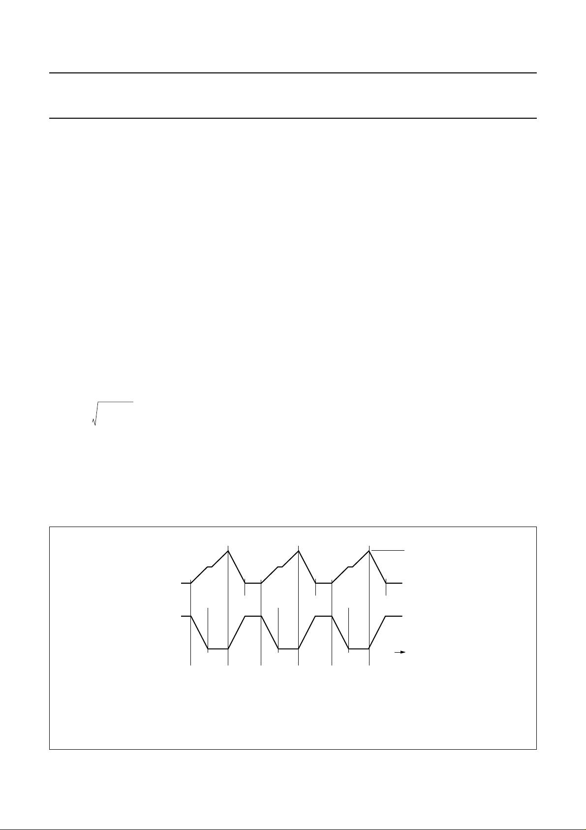
DAPTIVE COMMUTATION DELAY (CAP-CD AND CAP-DC)
In this circuit the capacitor CAP-CD is charged during one
commutation period, with an interruption of the charging
current during the diode pulse. During the next
commutation period the capacitor is discharged at twice
the charging current. The charging current is 8.1 µA and
the discharging current 16.2 µA; the voltage range is from
0.9 to 2.2 V. The voltage must stay within this range at the
lowest commutation frequency of interest, f
f 1.3×
6–
×
6231
------------ f
C1
(C in nF)
8.1 10
C
==
--------------------------
C1
:
If the commutation frequency is lower, a constant
commutation delay after the zero-crossing is generated by
the discharge from 2.2 down to 0.9 V at 16.2 µA;
maximum delay = (0.076 × C) ms (with C in nF)
Example: nominal commutation frequency = 900 Hz and
the lowest usable frequency = 400 Hz; so:
CAP-CD
6231
------------ 400
(choose 18 nF)
15.6==
The other capacitor, CAP-DC, is used to repeat the same
delay by charging and discharging with 15.5 µA. The same
value can be chosen as for CAP-CD. Figure 3 illustrates
typical voltage waveforms.
handbook, full pagewidth
voltage
on CAP-CD
(1)
(1) COM = commutation.
(2) ZCR = zero-crossing.
voltage
on CAP-DC
COMCOM
(2)
ZCRZCR
COM COM COM COM
ZCR ZCR ZCR ZCR
Fig.3 CAP-CD and CAP-DC typical voltage waveforms in normal running mode.
1997 Sep 12 6
V
= V
max
IH
V
IL
t
MGG993
 Loading...