


DATA SH EET
Product specification
Supersedes data of 1998 Apr 15
File under Integrated Circuits, IC02
1999 Oct 08
INTEGRATED CIRCUITS
TDA9901
Wideband differential digital
controlled variable gain amplifier
1999 Oct 08 2
Philips Semiconductors Product specification
Wideband differential digital controlled
variable gain amplifier
TDA9901
FEATURES
• 130 MHz, −3 dB small signal bandwidth
• Digitally controlled gain
• TTL/CMOS compatible digital inputs (3.3 or 5 V)
• TTL single ended or differential clock input with PECL
compatibility
• 24 dB gain control range
• Five steps of 6 dB plus 6 dB fixed gain
• 30 dB gain maximum
• High impedance differential inputs
• Low impedance differential outputs
• High power supply rejection
• 125 nV/√Hz output voltage noise density at 30 dB gain
• Fast gain settling
• Dual control modes: transparent or latched.
APPLICATIONS
• Linear AGC systems
• IF amplifierin IF conversion systems (e.g. base stations
or satellite receivers)
• Instrumentation
• Multi-purpose amplifier
• Driver for differential ADCs (e.g. TDA8768).
GENERAL DESCRIPTION
The TDA9901 is a wideband, low noise amplifier with
differential inputs andoutputs. TheTDA9901 incorporates
an AGC function with digital control. The TDA9901 is
optimized for fast switching between different gain
settings, preserving small phase and amplitude error.
The TDA9901 presents an excellent combination of low
noise and good linearity for a wide input frequency range.
The TDA9901 is optimized for processing IF signals in
GSM base stations. It is also suited for many other
applications as a general purpose digitally controlled
variable gain amplifier.
The TDA9901 is able to operate from 4.75 to 5.25 V
supply for the analog part and from 3.0 to 5.25 V for the
digital part.
QUICK REFERENCE DATA
ORDERING INFORMATION
SYMBOL PARAMETER CONDITIONS MIN. TYP. MAX. UNIT
V
DDA
analog supply voltage 4.75 5.0 5.25 V
V
DDD
digital supply voltage 3.0 3.3 5.25 V
I
DDA
analog supply current − 30 36 mA
I
DDD
digital supply current − 3.0 5.0 mA
G
dif
differential gain minimum gain 5.7 6.11 6.46 dB
maximum gain 29.3 30.5 31.5 dB
B
−3dB
−3 dB small signal bandwidth V
o(dif)(p-p)
= 0.125 V;
T
amb
=25°C
110 130 − MHz
P
tot
total power dissipation − 160 216 mW
TYPE
NUMBER
PACKAGE
NAME DESCRIPTION VERSION
TDA9901TS SSOP20 plastic shrink small outline package; 20 leads; body width 4.4 mm SOT266-1
1999 Oct 08 3
Philips Semiconductors Product specification
Wideband differential digital controlled
variable gain amplifier
TDA9901
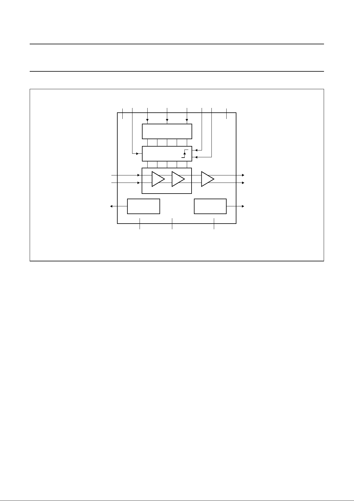
BLOCK DIAGRAM
Fig.1 Block diagram.
handbook, full pagewidth
MGM962
REFERENCE
GENERATOR
REFERENCE
GENERATOR
LATCHES
DECODER
GRAY2
19
GRAY1
20
V
SSD
17
V
SSA
12
165
7
6
14
15
n.c.
0, 6, 12, 18 or 24 dB
6 dB
8, 9, 10, 13
V
DDA
11
GRAY0
1
TE
2
V
DDD
18
CLK3CLKN
4
CMVGA
IN
INN
OUT
OUTN
CMADC
TDA9901
1999 Oct 08 4
Philips Semiconductors Product specification
Wideband differential digital controlled
variable gain amplifier
TDA9901
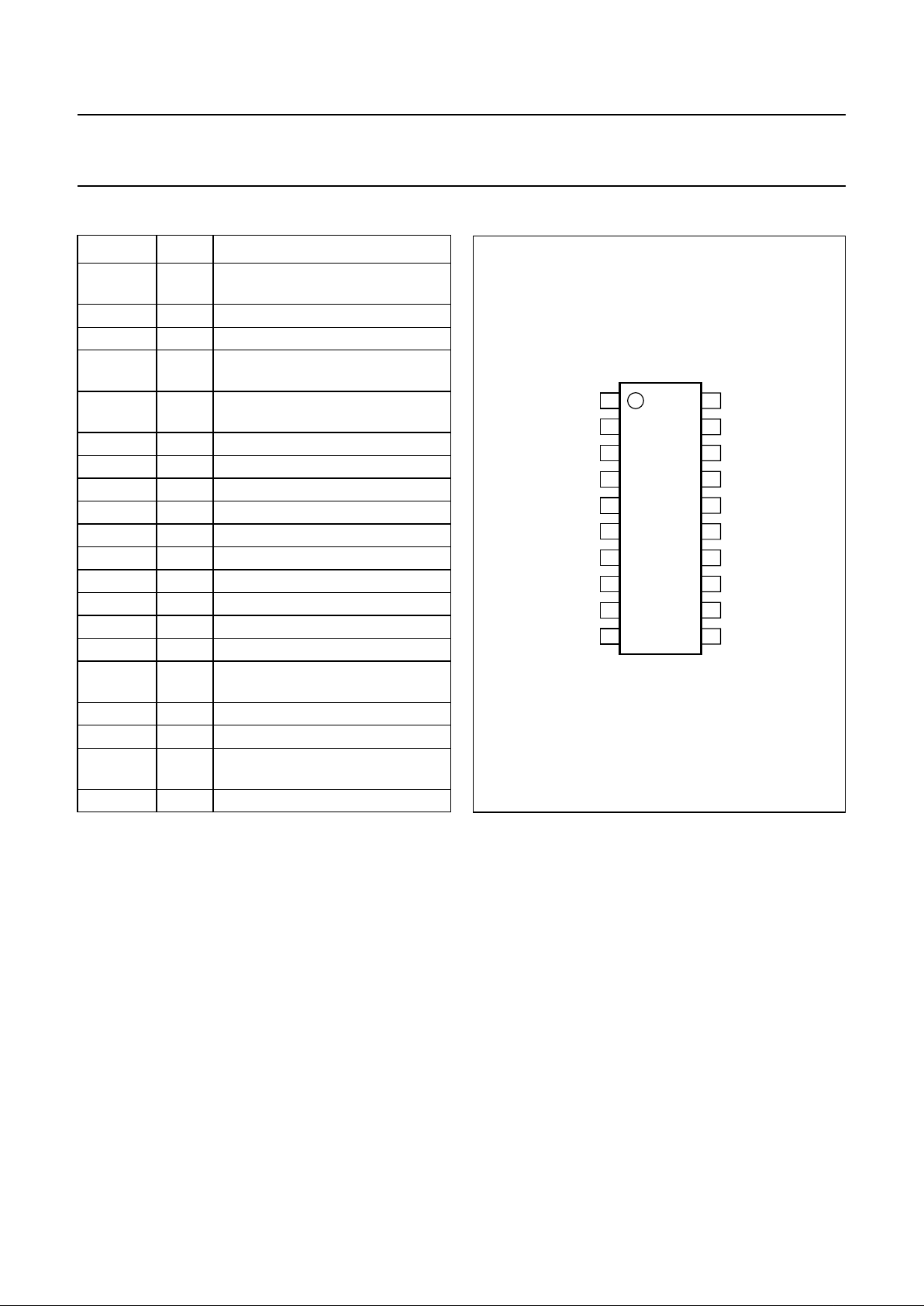
PINNING
SYMBOL PIN DESCRIPTION
GRAY0 1 digital control signal bit 0 input
(LSB)
TE 2 transparent enable input
CLK 3 clock input for gain control setting
CLKN 4 inverting clock input for gain
control setting (active low)
CMVGA 5 regulator output common mode
VGA input
IN 6 non-inverting analog input
INN 7 inverting analog input (active low)
n.c. 8 not connected
n.c. 9 not connected
n.c. 10 not connected
V
DDA
11 analog supply voltage
V
SSA
12 analog ground
n.c. 13 not connected
OUTN 14 inverting analog output (active low)
OUT 15 non-inverting analog output
CMADC 16 regulator output common mode
ADC input
V
SSD
17 digital ground
V
DDD
18 digital supply voltage
GRAY2 19 digital control signal bit 2 input
(MSB)
GRAY1 20 digital control signal bit 1 input
handbook, halfpage
GRAY0
TE
CLK
CLKN
CMVGA
IN
INN
n.c.
n.c.
n.c.
GRAY1
GRAY2
V
DDD
V
SSD
OUT
OUTN
CMADC
n.c.
V
SSA
V
DDA
1
2
3
4
5
6
7
8
9
10
11
12
20
19
18
17
16
15
14
13
TDA9901TS
MGM963
Fig.2 Pin configuration.
FUNCTIONAL DESCRIPTION
The TDA9901 provides a digitally controlled variable gain function for high-frequency applications.
The TDA9901 can beoperated in two different modes, depending onthe value at pin TE. When TE is at logic 1, the gain
can be instantly controlled when the clock signal is HIGH (transparent mode). The gain is fixed during the LOW period
of the clock. When TE is at logic 0 the gain of the TDA9901 is changed at the rising edge of the clock signal.
1999 Oct 08 5
Philips Semiconductors Product specification
Wideband differential digital controlled
variable gain amplifier
TDA9901
LIMITING VALUES
In accordance with the Absolute Maximum Rating System (IEC 134).
HANDLING
Inputs and outputs are protected against electrostatic discharges in normal handling. However, to be totally safe, it is
desirable to take normal precautions appropriate to handling integrated circuits.
THERMAL CHARACTERISTICS
CHARACTERISTICS
V
DDA=V11
to V12= 4.75 to 5.25 V; V
DDD=V18
to V17= 3.0 to 5.25 V; V
SSA
and V
SSD
shorted together;
T
amb
= −40 to +85 °C; typical values measured at V
DDA
= 5.0 V; V
DDD
= 3.3 V and T
amb
=25°C; unless otherwise
specified; note 1.
SYMBOL PARAMETER MIN. MAX. UNIT
V
DDA
analog supply voltage −0.3 +7.0 V
V
DDD
digital supply voltage −0.3 +7.0 V
∆V
DD
supply voltage difference between V
DDA
and V
DDD
−1.0 +4.0 V
V
I
input voltage level −0.3 +7.0 V
I
O
output current − 10 mA
T
stg
storage temperature −55 +150 °C
T
amb
ambient temperature −40 +85 °C
T
j
junction temperature − 150 °C
SYMBOL PARAMETER CONDITIONS VALUE UNIT
R
th(j-a)
thermal resistance from junction to ambient in free air 120 K/W
SYMBOL PARAMETER CONDITIONS MIN. TYP. MAX. UNIT
Supplies
V
DDA
analog supply voltage 4.75 5.0 5.25 V
V
DDD
digital supply voltage 3.0 3.3 5.25 V
∆V
DD
voltage difference
between V
DDA
and V
DDD
−0.2 − +2.5 V
I
DDA
analog supply current − 30 36 mA
I
DDD
digital supply current − 3.0 5.0 mA
Variable gain amplifier transfer characteristics
B
−3dB
−3 dB small signal
bandwidth
V
o(dif)(p-p)
= 0.125 V;
T
amb
=25°C
110 130 − MHz
t
d(g)
group delay time up to fi= 20 MHz;
minimum gain;
T
amb
=25°C
− 2.5 − ns
∆t
d(g)
group delay difference 6 dB gain step;
T
amb
=25°C
−−300 ps
1999 Oct 08 6
Philips Semiconductors Product specification
Wideband differential digital controlled
variable gain amplifier
TDA9901
t
st
settling time 10 to 90% maximum
output transition;
C
L(max)
= 5 pF on
each output;
T
amb
=25°C
−−3.6 ns
G
step
gain step size DC input
T
amb
=25°C 5.88 6.09 6.28 dB
all temperatures 5.6 6.09 6.56 dB
G
(min)
minimum gain setting DC input
T
amb
=25°C 5.76 6.11 6.40 dB
all temperatures 5.7 6.11 6.46 dB
G
(max)
maximum gain setting DC input
T
amb
=25°C 29.9 30.5 30.9 dB
all temperatures 29.3 30.5 31.5 dB
∆G/∆T gain stability as a function
of temperature
minimum gain −−1.0 − mdB/°C
maximum gain −−7.5 − mdB/°C
|∆G/∆VDD| gainstability as a function
of power supply
minimum gain − 15 25 mdB/V
∆V
i(offset)
input offset voltage
difference
6 dB gain step − 0.8 − mV
F noise figure R
s
= 100 Ω;
fi= 20 MHz
minimum gain − 29.1 − dB
maximum gain − 9.9 − dB
V
n(o)(eq)
equivalent output noise
voltage spectral density
Rs= 100 Ω;
fi= 20 MHz;
T
amb
=25°C
G=6dB − 75 − nV/√Hz
G = 12 dB − 82 − nV/√Hz
G = 18 dB − 97 − nV/√Hz
G = 24 dB − 91 − nV/√Hz
G = 30 dB − 124 − nV/√Hz
PSRR
(VDDA)
power supply ripple
rejection of V
DDA
minimum gain
0to20MHz − 57 − dB
20 to 100 MHz − 39 − dB
PSRR
(VDDD)
power supply ripple
rejection of V
DDD
minimum gain dB
0to20MHz − 67 − dB
20 to 100 MHz − 51 − dB
CMRR common mode rejection
ratio
0to20MHz − 75 − dB
20 to 150 MHz − 45 − dB
SYMBOL PARAMETER CONDITIONS MIN. TYP. MAX. UNIT
 Loading...