

Philips TDA9880-V1, TDA9880T-V1 Datasheet

DATA SH EET
Product specification
Supersedes data of 1998 Aug 12
File under Integrated Circuits, IC02
1999 Jul 21
INTEGRATED CIRCUITS
TDA9880
Alignment-freemultistandardvision
and FM sound IF-PLL demodulator

1999 Jul 21 2
Philips Semiconductors Product specification
Alignment-free multistandardvisionand
FM sound IF-PLL demodulator
TDA9880
FEATURES
• 5 V supply voltage
• Gain controlled wide-band Vision Intermediate
Frequency (VIF) amplifier (AC-coupled)
• True synchronous demodulation with active carrier
regeneration (very linear demodulation, good
intermodulation figures, reduced harmonics and
excellent pulse response)
• Fully integrated VIF Voltage Controlled Oscillator
(VCO), alignment-free
• Digital acquisition help, VIF frequencies of 38.0, 38.9,
45.75 and 58.75 MHz
• 4 MHz reference frequency input [signal from
Phase-Locked Loop (PLL) tuning system] or operating
as crystal oscillator
• VIF Automatic Gain Control (AGC) detector for gain
control, operating as peak sync detector, fast reaction
time
• Precise fullydigital Automatic Frequency Control (AFC)
detector with 4-bit digital-to-analog converter
• Fully integrated sound carrier trap for 4.5, 5.5,
6.0 and 6.5 MHz, controlled by reference signal
• Alignment-freeselectiveFM-PLL demodulator with high
linearity and low noise
• Digital frequency control, sound carrier frequencies
4.5, 5.5, 6.0 and 6.5 MHz
• Stabilizer circuit for ripple rejection and to achieve
constant output signals
• Electrostatic discharge (ESD) protection for all pins.
GENERAL DESCRIPTION
The TDA9880(T) is an integrated circuit for multistandard
vision IF signal processing and FM demodulation in TV
and VTR sets.
ORDERING INFORMATION
TYPE NUMBER
PACKAGE
NAME DESCRIPTION VERSION
TDA9880 SDIP20 plastic shrink dual in-line package; 20 leads (300 mil) SOT325-1
TDA9880T SO20 plastic small outline package; 20 leads; body width 7.5 mm SOT163-1

1999 Jul 21 3
Philips Semiconductors Product specification
Alignment-free multistandard vision and
FM sound IF-PLL demodulator
TDA9880
QUICK REFERENCE DATA
SYMBOL PARAMETER CONDITIONS MIN. TYP. MAX. UNIT
V
P
supply voltage note 1 4.5 5 5.5 V
I
P
supply current 85 100 115 mA
V
i(sens)(VIF)(rms)
VIF input voltage sensitivity
(RMS value)
−1 dB video at output − 50 100 µV
G
VIF(cr)
VIF gain control range see Fig.4 65 69 − dB
f
VIF
VIF frequencies see Table 2 − 38.0 − MHz
− 38.9 − MHz
− 45.75 − MHz
− 58.75 − MHz
∆f
VIF
VIF frequency window of digital
acquisition help
referenced to f
VIF
−±2.38 − MHz
V
o(v)(p-p)
video output signal voltage
(peak-to-peak value)
sound carrier off; see Fig.10 1.7 2.0 2.3 V
trap bypass mode;
see Fig.10
0.95 1.10 1.25 V
G
dif
differential gain
“NTC-7 Composite”
− 25%
ϕ
dif
differential phase
“NTC-7 Composite”
− 2 4 deg
B
v(−3dB)(trap)
−3 dB video bandwidth including
sound carrier trap
CL< 20 pF; RL>1kΩ;
AC load; note 2
f
trap
= 4.5 MHz
(M/N standard)
3.95 4.05 − MHz
f
trap
= 5.5 MHz
(B/G standard)
4.90 5.00 − MHz
α
SC1
trap attenuation at first sound carrier M/N standard 30 36 − dB
B/G standard 30 36 − dB
S/N
W
weighted signal-to-noise ratio of
video signal
see Fig.6; note 3 56 60 − dB
PSRR
13
power supply ripple rejection at
pin 13
f
ripple
= 70 Hz; video signal;
grey level; see Fig.9
25 28 − dB
B
v(−1dB)
−1 dB video bandwidth CL< 20 pF; RL>1kΩ;
AC load; trap bypass mode
56−MHz
I
ch(max)(20)
AGC maximum charge current at
pin 20
6810µA
I
dch(max)(20)
AGC maximum discharge current at
pin 20
7.5 10 12.5 µA
I
sink(14)
sink current of tuner AGC at pin 14 maximum tuner gain
reduction; V14=1V;
see Fig.4
450 600 750 µA
AFC
stps
AFC steepness ∆I19/∆f 0.85 1.05 1.25 µA/kHz
I
o(source)(19)
AFC output source current at pin 19 160 200 240 µA
I
o(sink)(19)
AFC output sink current at pin 19 160 200 240 µA
V
o(intc)(rms)
intercarrier output voltage
(RMS value)
; note 4
− 49 − mV
V
i(SC)
V
i(PC)
--------------
24 dB–=

1999 Jul 21 4
Philips Semiconductors Product specification
Alignment-free multistandard vision and
FM sound IF-PLL demodulator
TDA9880
Notes
1. Values of video and sound parameters can be decreased at VP= 4.5 V.
2. The sound carrier frequencies (depending on TV standard) are attenuated by the integrated sound carrier traps
(see Figs 13 to 18); H (s) is the absolute value of transfer function.
3. S/N is the ratio of black-to-white amplitude to the black level noise voltage (RMS value, pin 13). B = 4.2 MHz
(M/N standard) or B = 5.0 MHz (B/G, I and D/K standard) weighted in accordance with
“CCIR 567”
.
4. The intercarrier output signal at pin 11 can be calculated by the following formula taking into account the internal
video signal with 1.1 V (p-p) as a reference:
where:
= correction term for RMS value, = sound-to-picture carrier ratio at VIF input (pins 1 and 2) in dB,
6 dB = correction term of internal circuitry and ±3 dB = tolerance of video output and intercarrier output amplitude
V
o(intc)(rms)
.
B
intc(−3dB)(ul)
upper limit −3 dB intercarrier
bandwidth
7.5 9 − MHz
V
o(AF)(8)(rms)
audio output signal voltage at pin 8
(RMS value)
25 kHz FM deviation;
75 µs de-emphasis
400 500 600 mV
THD
8
total harmonic distortion at pin 8 − 0.15 0.5 %
B
AF(−3dB)
−3 dB audio frequency bandwidth without de-emphasis;
dependent on loop filter at
pin 4
100 120 − kHz
S/N
W(AF)
weighted signal-to-noise ratio of
audio signal
black picture 50 56 − dB
white picture 45 51 − dB
6 kHz sine wave
(black-to-white modulation)
40 46 − dB
sound carrier
subharmonics;
f = 2.25 MHz ±3 kHz
35 40 − dB
α
AM(sup)
AM suppression of FM demodulator 75 µs de-emphasis;
AM: f = 1 kHz; m = 0.3
referenced to 25 kHz
FM deviation
40 46 − dB
PSRR
8
power supply ripple rejection at pin 8 f
ripple
= 70 Hz; see Fig.9 14 20 − dB
∆f
FM
frequency window of digital
acquisition help for FM demodulator
−±225 − kHz
f
ref(15)
frequency of reference signal at
pin 15
− 4.0 − MHz
V
ref(15)(rms)
amplitude of referencesignal source
at pin 15 (RMS value)
operation as input terminal 80 − 400 mV
SYMBOL PARAMETER CONDITIONS MIN. TYP. MAX. UNIT
V
o(intc)(rms)
1.1 V (p-p)
1
22
---------- -
× 10
V
iSC()
V
iPC()
---------------
dB()6 dB 3 dB±+
20
--------------------------------------------------------------- -
×=
1
22
---------- -
V
iSC()
V
iPC()
---------------
dB()
1999 Jul 21 5
Philips Semiconductors Product specification
Alignment-free multistandard vision and
FM sound IF-PLL demodulator
TDA9880
This text is here in white to force landscape pages to be rotated correctly when browsing through the pdf in the Acrobat reader.This text is here in
_white to force landscape pages to be rotated correctly when browsing through the pdf in the Acrobat reader.This text is here inThis text is here in
white to forcelandscapepagesto be rotated correctly when browsing through the pdf in the Acrobat reader. white to force landscape pages to be ...
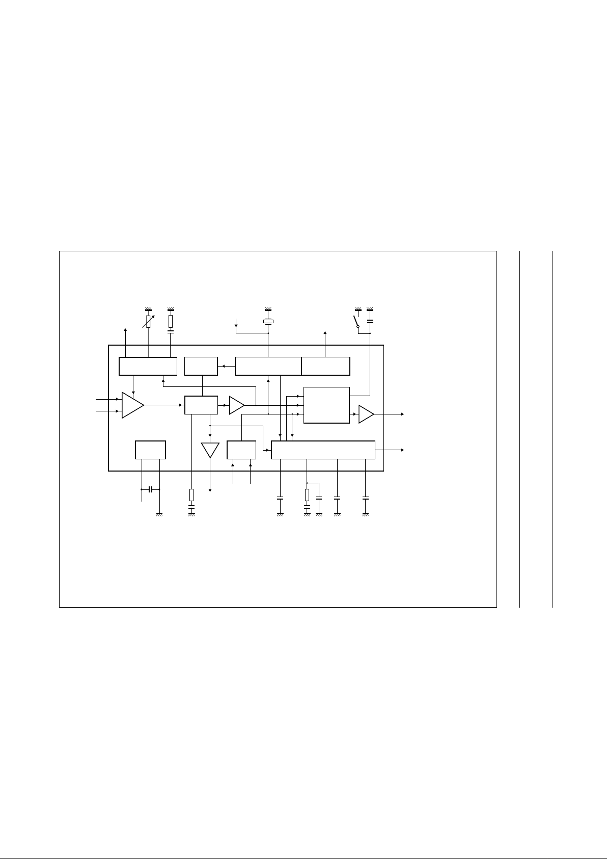
BLOCK DIAGRAM
d
book, full pagewidth
MHB506
DIGITAL VCO CONTROL AFC DETECTOR
RC VCO
VIF-PLL
AGC
SUPPL Y
LOGIC
NARROW-BAND FM-PLL DETECTOR
SOUND TRAPS
4.5 to 6.5 MHz
TAGC
C
VAGC
VAGC
R
TOP
TOP
14 3 20 15 19 12
645710
911181617
1
2
13
8
external reference
or 4 MHz crystal
REF
AFC
TR
C
TR
trap disable
switch
CVBS
AUD
audio output
video output 2 V (p-p)
[1.1 V (p-p) without trap]
C
AFD
C
FAGC
FAGC
SIO
S1S0
VPLLVPGND
FMPLL DEEM AFD
C
DEEM
sound
intercarrier
output
VIF-PLL
filter
FM-PLL
filter
de-emphasis decoupling
VIF1
VIF2
TDA9880
Fig.1 Block diagram.
1999 Jul 21 6
Philips Semiconductors Product specification
Alignment-free multistandard vision and
FM sound IF-PLL demodulator
TDA9880
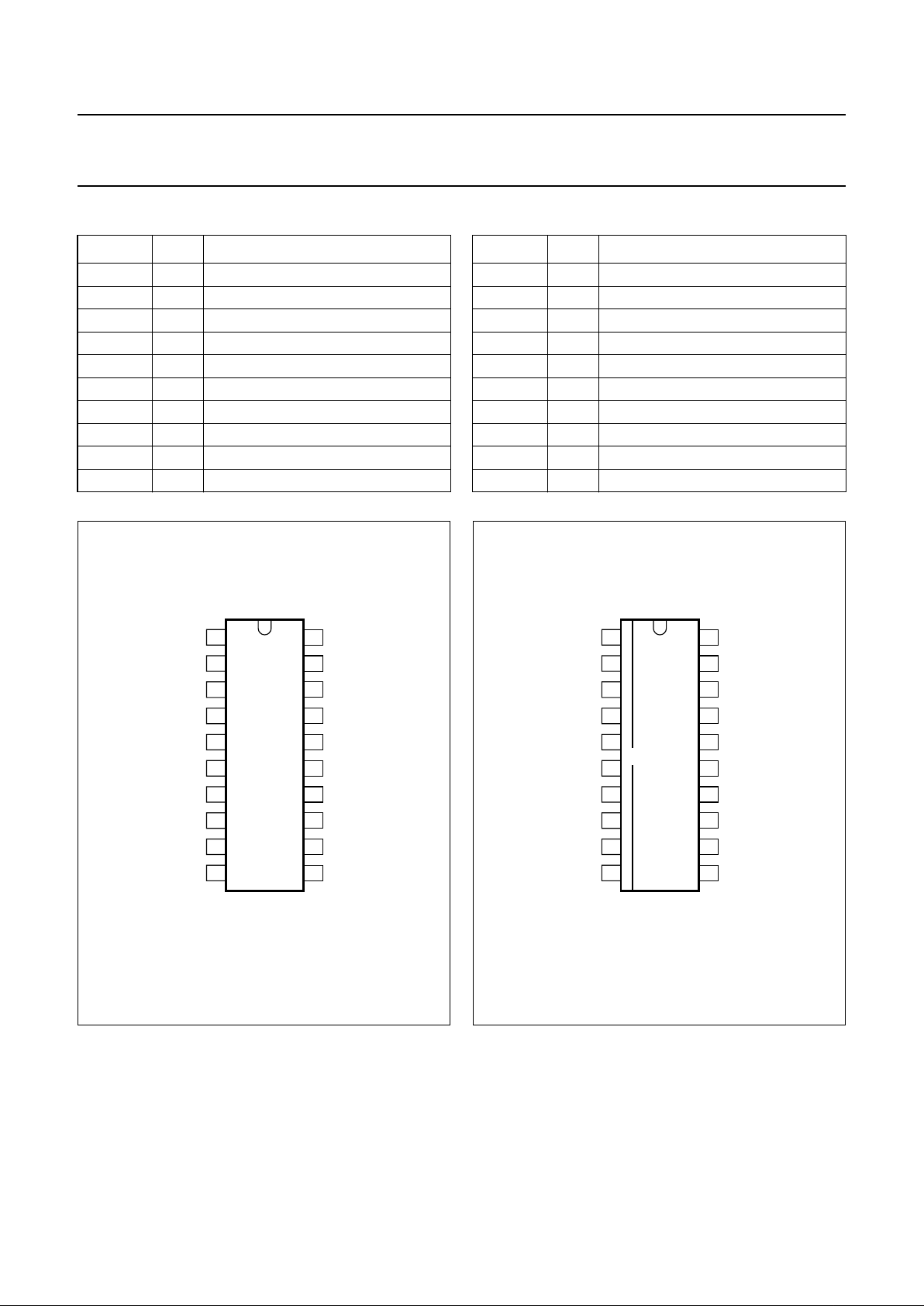
PINNING
SYMBOL PIN DESCRIPTION
VIF1 1 VIF differential input 1
VIF2 2 VIF differential input 2
TOP 3 tuner AGC TakeOver Point (TOP)
FMPLL 4 FM-PLL filter
DEEM 5 de-emphasis capacitor
AFD 6 AF decoupling capacitor
FAGC 7 FM-PLL AGC capacitor
AUD 8 audio output
S0 9 switch input S0
S1 10 switch input S1
SIO 11 sound intercarrier output
TR 12 trap control
CVBS 13 video output
TAGC 14 tuner AGC output
REF 15 4 MHz crystal or reference input
GND 16 ground supply
V
P
17 supply voltage (+5 V)
VPLL 18 VIF-PLL filter
AFC 19 AFC output
VAGC 20 VIF-AGC capacitor
SYMBOL PIN DESCRIPTION
Fig.2 Pin configuration for SDIP20.
handbook, halfpage
VIF1
VIF2
TOP
FMPLL
DEEM
AFD
FAGC
AUD
S0
S1
VAGC
AFC
VPLL
V
P
REF
TAGC
GND
CVBS
TR
SIO
1
2
3
4
5
6
7
8
9
10
11
12
20
19
18
17
16
15
14
13
TDA9880
MHB072
Fig.3 Pin configuration for SO20.
handbook, halfpage
VIF1
VIF2
TOP
FMPLL
DEEM
AFD
FAGC
AUD
S0
S1
VAGC
AFC
VPLL
V
P
REF
TAGC
GND
CVBS
TR
SIO
1
2
3
4
5
6
7
8
9
10
11
12
20
19
18
17
16
15
14
13
TDA9880T
MHB106

1999 Jul 21 7
Philips Semiconductors Product specification
Alignment-free multistandard vision and
FM sound IF-PLL demodulator
TDA9880
FUNCTIONAL DESCRIPTION
Figure 1 shows the simplified block diagram of the
integrated circuit. The integrated circuit comprises the
following functional blocks:
1. VIF amplifier
2. Tuner-AGC and VIF-AGC
3. VIF-AGC detector
4. Frequency Phase-Locked Loop (FPLL) detector
5. VCO and Travelling Wave Divider (TWD)
6. Digital acquisition help and AFC
7. Video demodulator and amplifier
8. Sound carrier trap
9. Intercarrier mixer
10. FM demodulator and acquisition help
11. Audio amplifier
12. Internal voltage stabilizer.
VIF amplifier
The VIF amplifier consists of three AC-coupled differential
amplifier stages. Each differential stage comprises a
feedback network controlled by emitter degeneration.
Tuner-AGC and VIF-AGC
The AGC capacitor voltage is converted to an internal VIF
gaincontrol signal, and is fedto the tuner AGC togenerate
the tuner AGC output current at pin TAGC (open-collector
output). The tuner AGC takeover point can be adjusted
with R
TOP
. This allows the tuner to be matchedto the SAW
filter in order to achieve the optimum IF input level.
VIF-AGC detector
The AGC detector generates the required VIF gain control
voltage for constant video output by charging or
discharging the AGC capacitor. Gain control is performed
by sync level detection. The newly developed AGC circuit
provides fast reaction time to cope with ‘aeroplane
fluttering’. The time constants for decreasing or increasing
gain are nearly equal.
Frequency Phase-Locked Loop (FPLL) detector
The VIF amplifier output signal is fed into a Frequency
Detector(FD) and into a PhaseDetector (PD) via a limiting
amplifier. During acquisition the frequency detector
produces a DC current proportional to the frequency
difference between the input and the VCO signal.
After frequency lock-in the phase detector produces a DC
current proportional to the phase difference between the
VCO and the input signal. The DC current of either the
frequency detector or the phase detector is converted into
aDCvoltagevia the VIF-PLL filter, which controls the VCO
frequency.
VCO and Travelling Wave Divider (TWD)
The Resistor Capacitor (RC) VCO operates as an
integrated relaxation oscillator atdouble the picture carrier
frequency.The control voltage required totunethe VCO to
actually double the picture carrier frequency is generated
by the FPLL detector and fed via the loop filter to the VCO
control input terminal.
The oscillator signal is divided-by-two with a TWD which
generatestwo differential output signals witha 90 degrees
phase difference independent of the frequency.
Digital acquisition help and AFC
The integrated relaxation oscillator has a very wide
frequency range from approximately 30 to 70 MHz (after
the TWD). To prevent false locking of the FPLL and with
respect to the catching range of the frequency detector of
maximum ±2.5 MHz, the Digital Acquisition Help (DAH)
provides current into the loop filter until the VCO is in a
frequency window of ±2.3 MHz around the wanted VIF
frequency. In this case the analog operating FPLL willlock
the VCO to the VIF carrier and the acquisition help does
not provide any current to the loop filter.
The principle of the digital acquisition help is as follows:
the VCO is connected to a downcounter, which is preset
depending on the required VIF frequency. The counting
time, as well as the counter control, is derived from a
4 MHz reference signal. This signal can be supplied from
the internal 4 MHz crystal oscillator or from the 4 MHz
reference oscillator of an external tuning system.
The counting result after a counting cycle corresponds to
the actual VCO frequency.
The digital AFC is also derived from the counting result
after a counting cycle by digital-to-analog converting the
last four bits of the counter.
Video demodulator and amplifier
The video demodulator is realized by a multiplier which is
designedforlowdistortionandlargebandwidth.Thevision
IF input signal is multiplied with the ‘in phase’ signal of the
travelling wave divider output.

1999 Jul 21 8
Philips Semiconductors Product specification
Alignment-free multistandard vision and
FM sound IF-PLL demodulator
TDA9880
The demodulator output signal is fed via an integrated
low-pass filter for attenuation of the carrier harmonics to
the video amplifier. The video amplifier is realized by an
operational amplifier with internal feedback and high
bandwidth. A low-pass filter is integrated to achieve an
attenuation of the carrier harmonics. The video signal of
1.1 V (p-p) for nominal vision IF modulation is fed
internally to the integrated sound carrier trap as well as to
the VIF-AGC detector. The second stage of the video
amplifier converts and amplifies the differential output
signal from the sound carrier trap to the single-ended
CVBS output signal at pin 13 with a 2 V (p-p) amplitude.
Noise clipping is provided. Furthermore the trap can be
bypassed by the implemented input switch of the second
amplifier stage, forced by connecting pin 12 to ground.
Sound carrier trap
The sound carrier trap consists of a reference filter, a
phase detector and the sound trap itself.
A sound carrier reference signal is fed into the reference
low-pass filter and is shifted by a nominal 90 degrees.
The phasedetectorcomparestheoriginalreferencesignal
with the signal shiftedby the reference filter and produces,
at the external capacitor CTR, a DC voltage by charging or
discharging the capacitor with a current proportional to the
phase difference between both signals, respectively to the
frequency error of the integrated filters. The DC voltage is
converted to currents which control the frequency position
of the reference filter and the sound trap.
The sound trap itselfis constructed of three separate traps
to realize sufficient suppression of the first and second
sound carrier. The right frequency position of the different
standards is set by the sound carrier reference signal.
Intercarrier mixer
The intercarrier mixer is realized by a multiplier, operating
inquadraturemodeforsuppressionoflowfrequencyvideo
signals. The VIF amplifier output signal is fed to the
intercarrier mixer and converted to an intercarrier
frequency by the regenerated 90 degree picture carrier
from the VCO. The mixer output signal is fed via a
band-pass filter and amplifier for attenuation of the high
frequency video signal components and carrier harmonics
to the output pin 11. The intercarrier signal is fed also to
the integrated FM demodulator.
FM demodulator and acquisition help
The FM demodulator is realized as a narrow-band PLL
with external loop filter, which provides the necessary
selectivity. To achieve good selectivity, a linear phase
detector and constant input level are required.
The intercarrier signal from the intercarrier mixer is fed via
a gain controlled amplifier to the phase detector and it’s
output signal controls (via the loop filter) the integrated
relaxation oscillator. The possible frequency range is from
4 to 7 MHz. As a result of locking the oscillator frequency
tracks with the FM modulation of the input signal;
therefore,theoscillator control voltage is superimposed by
the AF voltage. In this way the FM-PLL operates as an
FM demodulator. The AF voltage is present at the loop
filter and is fed via a buffer with 0 dB gain to the audio
amplifier.
The digital acquisition help operates in the same way as
described in Section “Digital acquisition help and AFC”.
Audio amplifier
The audio amplifier consists of two parts:
1. The AF preamplifier is an operational amplifier with
internal feedback, high gain and high common mode
rejection. The AF voltage from the PLL demodulator,
by principle a small output signal, is amplified by
30 dB. A DC operating point control circuit (pin 6)
decouples the AF amplifier from the DC voltage of the
PLL. The low-pass characteristic of the amplifier
reduces the harmonics of the intercarrier signal at the
sound output terminal. If required, a de-emphasis
network can be realized by the amplifier output
resistance and an external capacitor.
2. The AF output amplifier (10 dB) provides the required
output level by a rail-to-rail output stage. This amplifier
makes use of an input selector for switching to mute
state, automatically controlled by the mute switching
voltage from the digital acquisition help in order to
avoid lock-in noise. During normal operation the
automatic audio mute function is not active.
Application of a 2.2 kΩ resistor between the
intercarrier output (pin 11)and ground will activate the
automatic audio mute function.
Internal voltage stabilizer
The band gap circuit internally generates a voltage of
approximately 2.4 V, independent of the supply voltage
and the temperature. Avoltage regulator circuit, controlled
by this voltage, produces a constant voltage of 3.55 V
which is used as an internal reference voltage.

1999 Jul 21 9
Philips Semiconductors Product specification
Alignment-free multistandard vision and
FM sound IF-PLL demodulator
TDA9880
LIMITING VALUES
In accordance with the Absolute Maximum Rating System (IEC 134).
Notes
1. Charge device model class A; machine model: discharging a 200 pF capacitor via a 0.75 µH inductance.
2. Charge device model class B; human body model: discharging a 100 pF capacitor via a 1.5 kΩ series resistor.
THERMAL CHARACTERISTICS
SYMBOL PARAMETER CONDITIONS MIN. MAX. UNIT
V
P
supply voltage IP= 115 mA; T
amb
=70°C; at
maximum chip temperature of 125 °C
− 5.5 V
V
n
voltage at
pins 1 to 4, 6 to 10, 12 and 17 to 20 0 V
P
V
pin 14 0 13.2 V
t
sc
short-circuit time to ground or V
P
− 10 s
T
stg
storage temperature −25 +150 °C
T
amb
ambient temperature −20 +70 °C
V
es
electrostatic handling voltage for all
pins
note 1 −250 +250 V
note 2 −3000 +3000 V
SYMBOL PARAMETER CONDITIONS VALUE UNIT
R
th(j-a)
thermal resistance from junction to ambient in free air
TDA9880 (SDIP20) 85 K/W
TDA9880T (SO20) 85 K/W
1999 Jul 21 10
Philips Semiconductors Product specification
Alignment-free multistandard vision and
FM sound IF-PLL demodulator
TDA9880
CHARACTERISTICS
VP=5V; T
amb
=25°C; see Table 2 for input frequencies; M standard (fPC= 45.75 MHz; fSC= 41.25 MHz;
PC/SC = 10 dB) is used for specification; V
i(VIF)(rms)
= 10 mV (sync level); IF input from 50 Ω via broadband transformer
1 : 1; DSB video modulation; 10% residual carrier; video signal in accordance with
“NTC-7 Composite”
; measurements
taken in test circuit of Fig.19; unless otherwise specified.
SYMBOL PARAMETER CONDITIONS MIN. TYP. MAX. UNIT
Supply (pin 17)
V
P
supply voltage note 1 4.5 5 5.5 V
I
P
supply current 85 100 115 mA
P
tot
total power dissipation − 500 633 mW
VIF amplifier (pins 1 and 2)
V
i(sens)(VIF)(rms)
VIF input voltage sensitivity
(RMS value)
−1 dB video at output − 50 100 µV
V
i(max)(rms)
maximum input signal voltage
(RMS value)
1 dB video at output;
note 2
110 −−mV
∆V
int
internal IF amplitudedifference
between picture and sound
carrier
within AGC range;
∆f = 4.5 MHz
− 0.7 1 dB
G
VIF(cr)
VIF gain control range see Fig.4 65 69 − dB
B
VIF(−3dB)(ll)
lower limit −3 dB VIF
bandwidth
− 15 25 MHz
B
VIF(−3dB)(ul)
upper limit −3 dB VIF
bandwidth
70 100 − MHz
R
i(dif)
differential input resistance note 3 1.7 2.2 2.7 kΩ
C
i(dif)
differential input capacitance note 3 1.2 1.7 2.5 pF
V
I
DC input voltage − 3.35 − V
FPLL and true synchronous video demodulator; note 4
f
VCO(max)
maximum oscillator frequency
for carrier regeneration
f=2f
PC
120 140 − MHz
f
VIF
vision carrier operating
frequencies
see Table 2 − 38.0 − MHz
− 38.9 − MHz
− 45.75 − MHz
− 58.75 − MHz
∆f
VIF
VIFfrequency window of digital
acquisition help
referenced to f
VIF
−±2.38 − MHz
t
acq
acquisition time BL = 70 kHz; note 5 −−30 ms
V
i(sens)(VIF)(rms)
VIF input voltage sensitivity at
pins 1 and 2 (RMS value)
for PLL to be locked maximum IF gain − 30 70 µV
for C/N = 10 dB notes 6 and 7 − 100 140 µV
SIGNAL AT PIN 18
I
o(source)(PD)(max)
maximum source current of
phase detector output
− 17 −µA

1999 Jul 21 11
Philips Semiconductors Product specification
Alignment-free multistandard vision and
FM sound IF-PLL demodulator
TDA9880
I
o(sink)(PD)(max)
maximum sink current of
phase detector output
− 17 −µA
I
o(source)(DAH)
output source current of digital
acquisition help
− 23 −µA
I
o(sink)(DAH)
output sink current of digital
acquisition help
− 23 −µA
t
W(min)(DAH)
minimum pulse width of digital
acquisition help current
− 64 −µs
K
O(VIF)
VCO steepness ∆f
VIF
/∆V
18
− 20 − MHz/V
K
D(VIF)
phase detector steepness
∆I18/∆ϕ
VIF
− 23 −µA/rad
Video output signal and sound carrier trap (pin 13; sound carrier off)
V
o(v)(p-p)
video output signal voltage
(peak-to-peak value)
see Fig.10 1.7 2.0 2.3 V
V
sync
sync pulse voltage level see Fig.10 1.15 1.35 1.55 V
V
zc
zero carrier voltage level see Fig.10 3.27 3.57 3.87 V
V
v(clu)
upper video clipping voltage
level
VP− 1.1 VP− 1 − V
V
v(cll)
lower video clipping voltage
level
− 0.7 1.0 V
R
o
output resistance note 3 −−30 Ω
I
bias(int)
internal DC bias current for
emitter-follower
2.0 2.5 − mA
I
o(source)(max)
maximum AC and DC output
source current
2.4 −−mA
I
o(sink)(max)
maximum AC and DC output
sink current
1.4 −−mA
∆V
o
deviation of CVBS output
signal voltage
50 dB gain control −−0.5 dB
30 dB gain control −−0.1 dB
∆V
o(bl)
black level tilt −−1%
G
dif
differential gain
“NTC-7 Composite”
− 25%
ϕ
dif
differential phase
“NTC-7 Composite”
− 2 4 deg
B
v(−3dB)(trap)
−3 dB video bandwidth
including sound carrier trap
CL< 20 pF; RL>1kΩ;
AC load; note 8
f
trap
= 4.5 MHz
(M/N standard)
3.95 4.05 − MHz
f
trap
= 5.5 MHz
(B/G standard)
4.90 5.00 − MHz
f
trap
= 6.0 MHz
(I standard)
5.2 5.50 − MHz
f
trap
= 6.5 MHz
(D/K standard)
5.5 5.95 − MHz
SYMBOL PARAMETER CONDITIONS MIN. TYP. MAX. UNIT

1999 Jul 21 12
Philips Semiconductors Product specification
Alignment-free multistandard vision and
FM sound IF-PLL demodulator
TDA9880
α
SC1
trap attenuation at first sound
carrier
M/N standard 30 36 − dB
B/G standard 30 36 − dB
I standard 26 32 − dB
D/K standard 26 32 − dB
α
SC1(60 kHz)
trap attenuation at first sound
carrier f
SC1
±60 kHz
M/N standard 21 27 − dB
B/G standard 24 30 − dB
I standard 20 26 − dB
D/K standard 20 26 − dB
α
SC2
trap attenuation at second
sound carrier
M/N standard 21 27 − dB
B/G standard 21 27 − dB
I standard 12 18 − dB
D/K standard 18 24 − dB
α
SC2(60 kHz)
trap attenuation at second
sound carrier f
SC2
±60 kHz
M/N standard 15 21 − dB
B/G standard 15 21 − dB
I standard 10 15 − dB
D/K standard 13 18 − dB
t
d(g)(CC)
group delay at chrominance
carrier frequency
3.58 MHz at
M/N standard
110 180 250 ns
4.43 MHz at B/G standard 110 180 250 ns
4.43 MHz at I standard − 90 160 ns
4.28 MHz at D/K standard − 60 130 ns
S/N
W
weighted signal-to-noise ratio weighted in accordance
with
“CCIR 567”
;
see Fig.6; note 9
56 60 − dB
S/N
UW
unweighted signal-to-noise
ratio
note 9 47 51 − dB
αd
blue
intermodulation attenuation at
‘blue’
f = 0.92 MHz; see Fig.7;
note 10
58 64 − dB
f = 2.76 MHz; see Fig.7;
note 10
58 64 − dB
αd
yellow
intermodulation attenuation at
‘yellow’
f = 0.92 MHz; see Fig.7;
note 10
60 66 − dB
f = 2.76 MHz; see Fig.7;
note 10
59 65 − dB
∆V
r(vc)(rms)
residual vision carrier
(RMS value)
fundamental wave and
harmonics
− 25mV
α
H(sup)
harmonics suppression in
video signal
CL< 20 pF; RL>1kΩ;
AC load; note 11a
35 40 − dB
α
H(spur)
spuriouselements suppression
in video signal
note 11b 40 −−dB
PSRR
13
powersupply ripple rejectionat
pin 13
f
ripple
= 70 Hz; video
signal; grey level;
see Fig.9
25 28 − dB
SYMBOL PARAMETER CONDITIONS MIN. TYP. MAX. UNIT
 Loading...