

Philips TDA9874APS-V2, TDA9874AH-V2 Datasheet

DATA SH EET
Preliminary specification
File under Integrated Circuits, IC02
1999 Dec 03
INTEGRATED CIRCUITS
TDA9874A
Digital TV sound
demodulator/decoder

1999 Dec 03 2
Philips Semiconductors Preliminary specification
Digital TV sound demodulator/decoder TDA9874A
CONTENTS
1 FEATURES
2 GENERAL DESCRIPTION
2.1 Supported standards
3 ORDERING INFORMATION
4 BLOCK DIAGRAM
5 PINNING
6 FUNCTIONAL DESCRIPTION
6.1 Description of the demodulator and decoder
section
6.2 Description of the DSP
6.3 Description of the analog audio section
7 LIMITING VALUES
8 THERMAL CHARACTERISTICS
9 CHARACTERISTICS
10 I2C-BUS CONTROL
10.1 Introduction
10.2 Power-up state
10.3 Slave receiver mode
10.4 Slave transmitter mode
11 I2S-BUS DESCRIPTION
12 EXTERNAL COMPONENTS
13 PACKAGE OUTLINES
14 SOLDERING
14.1 Introduction
14.2 Through-hole mount packages
14.3 Surface mount packages
14.4 Suitability of IC packages for wave,reflow and
dipping soldering methods
15 DEFINITIONS
16 LIFE SUPPORT APPLICATIONS
17 PURCHASE OF PHILIPS I2C COMPONENTS

1999 Dec 03 3
Philips Semiconductors Preliminary specification
Digital TV sound demodulator/decoder TDA9874A
1 FEATURES
• Sound IF (SIF) input switch
• SIF AGC with 24 dB control range
• Switchable 10 dB SIF input attenuator
• SIF 8-bit Analog-to-Digital Converter (ADC)
• Easy TV standard programming option
• Differential Quadrature Phase Shift Keying (DQPSK)
demodulation for different standards, simultaneously
with 1-channel FM demodulation
• NICAM decoding (B/G, D/K, I and L standard)
• 2-carriermulti-standardFMdemodulation(B/G,D/Kand
M standard)
• Single carrier high deviation FM mono demodulation
mode
• Decoding for three analog multi-channel systems (A2)
and satellite sound
• Adaptive de-emphasis for satellite
• Programmable identification (B/G, D/K and M standard)
and different identification times
• FM pilot carrier presence detector
• OptionalAMdemodulationforsystem L, simultaneously
with NICAM
• Monitor selection for FM/AM demodulator outputs and
FM and NICAM signals with peak option
• Automatic FM dematrixing option
• Digital crossbar switch
• I2S-bus serial audio output with matrix, level adjustment
and mute
• Dual audio Digital-to-Analog Converter (DAC) from
digital crossbar switch to analog crossbar switch,
bandwidth = 15 kHz
• Automatic Volume Level (AVL) control
• Analog crossbar switch with inputs for mono and stereo
• Output selection of mono, stereo, dual, dual A or dual B
• Additional mono output with automatic select
• 20 kHz bandwidth for analog path
• Standby mode
• Automatic output selection for TV applications.
2 GENERAL DESCRIPTION
The TDA9874A is a single-chip Digital TV Sound
Demodulator/Decoder (DTVSD) for analog and digital
multi-channel sound systems in TV/VCR sets and satellite
receivers.
2.1 Supported standards
The multi-standard/multi-stereo capability of the
TDA9874A is of interest in Europe, Hong Kong/PR China
and South East Asia. This includes B/G, D/K, I, M and
L standard. In other application areas subsets of the
standard combinations are available or, only single
standards are transmitted.
All A2 (analog 2-carrier) and NICAM systems are
supported. M standard (with mono or BTSC stereo sound)
can be received and processed in mono sound mode.
The AM sound of L/L’ standard is normally demodulated in
the1st soundIF.The resulting AF signal has to be entered
into the mono audio input of the TDA9874A. A second
possibility is to use the internal AM demodulator stage
(with 6.5 MHz intercarrier), which gives limited
performance.
Korea has a stereo sound system similar to Europe and is
supported by the TDA9874A. The differences include
deviation, modulation contents and identification. It is
based on M standard.
For all FM standards a high deviation mode for a single
carrier monaural sound demodulation is selectable.
An overview of the supported standards and sound
systems and their key parameters is given in
Tables 1 to 3.
The analog multi-channel systems are sometimes also
called 2CS (2-carrier systems).
1999 Dec 03 4
Philips Semiconductors Preliminary specification
Digital TV sound demodulator/decoder TDA9874A
2.1.1 ANALOG 2-CARRIER SYSTEMS
Table 1 Frequency modulation
Table 2 Identification for A2 systems
2.1.2 2-
CARRIER SYSTEMS WITH NICAM
Table 3 NICAM
Notes
1. See
“EBU NICAM 728 specification”
or equivalent specification.
2. Not yet officially defined.
STANDARD
SOUND
SYSTEM
CARRIER
FREQUENCY
(MHz)
FM DEVIATION (kHz) MODULATION BANDWIDTH/
DE-EMPHASIS
(kHz/µs)
NOM. MAX. OVER. SC1 SC2
M mono 4.5 15 25 50 mono − 15/75
M A2 4.5/4.724 15 25 50
1
⁄2(L+R)1⁄2(L − R) 15/75 (Korea)
B/G A2 5.5/5.742 27 50 80
1
⁄2(L + R) R 15/50
I mono 6.0 27 50 80 mono − 15/50
D/K (2) A2 6.5/6.742 27 50 80
1
⁄2(L + R) R 15/50
D/K (1) A2 6.5/6.258 27 50 80
1
⁄2(L + R) R 15/50
D/K (3) A2 6.5/5.742 27 50 80
1
⁄2(L + R) R 15/50
PARAMETER A2; A2* A2+ (KOREA)
Pilot frequency 54.6875 kHz = 3.5 × line frequency 55.0699 kHz = 3.5 × line frequency
Stereo identification frequency
Dual identification frequency
AM modulation depth 50% 50%
STANDARD
SC1
SC2
(MHz)
NICAM
DE-
EMPHASIS
ROLL-
OFF (%)
NICAM
CODING
FREQUENCY
(MHz)
TYPE
MODULATION
INDEX (%)
DEVIATION
(kHz)
NOM. MAX. NOM. MAX.
B/G 5.5 FM −−27 50 5.85 J17 40 note 1
I 6.0 FM −−27 50 6.552 J17 100 note 1
D/K 6.5 FM −−27 50 5.85 J17 40 note 2
L 6.5 AM 54 100 −−5.85 J17 40 note 1
117.5 Hz
line frequency
133
-------------------------------------- -
= 149.9 Hz
line frequency
105
-------------------------------------- -
=
274.1 Hz
line frequency
57
-------------------------------------- -
= 276.0 Hz
line frequency
57
-------------------------------------- -
=

1999 Dec 03 5
Philips Semiconductors Preliminary specification
Digital TV sound demodulator/decoder TDA9874A
2.1.3 SATELLITE SYSTEMS
An important specification for satellite TV reception is the Astra specification. The TDA9874A is suitable for the reception
of Astra and other satellite signals, with sound carrier frequencies from 4 to 9.2 MHz.
Table 4 FM satellite sound
Notes
1. Forothersatellite systems, frequencies of e.g. 5.80, 6.60 or 6.65 MHz can alsobereceived.A de-emphasis of 60 µs,
or in accordance with J17, is available.
2. Main channels with high deviation can also be handled.
3. m/st/d = mono or stereo or dual language sound.
4. Adaptive de-emphasis is compatible to transmitter specification.
3 ORDERING INFORMATION
CARRIER TYPE
CARRIER
FREQUENCY
(MHz)
MODULATION
INDEX
MAXIMUM
FM DEVIATION
(kHz)
MODULATION
BANDWIDTH/
DE-EMPHASIS
(kHz/µs)
Main 6.50
(1)
0.26 85
(2)
mono 15/50
(1)
Sub 7.02/7.20 0.15 50 m/st/d
(3)
15/adaptive
(4)
7.38/7.56
7.74/7.92
8.10/8.28
TYPE NUMBER
PACKAGE
NAME DESCRIPTION VERSION
TDA9874APS SDIP42 plastic shrink dual in-line package; 42 leads (600 mil) SOT270-1
TDA9874AH QFP44 plasticquad flat package; 44 leads (lead length 2.35 mm);
body 14 × 14 × 2.2 mm
SOT205-1
1999 Dec 03 6
Philips Semiconductors Preliminary specification
Digital TV sound demodulator/decoder TDA9874A
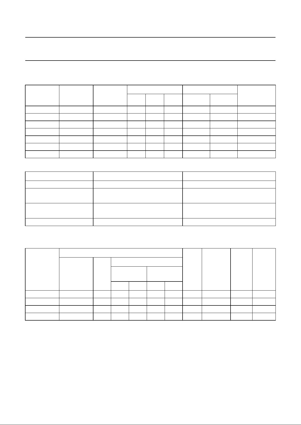
4 BLOCK DIAGRAM
handbook, full pagewidth
MHB584
NICAM
DEMODULATION
FM/AM
DEMODULATION
NICAM
DECODER
2-CHANNEL
ANALOG/
SATELLITE
DECODER
POST FILTER
3 DACs
SUPPLY
DACs
OPAMPS
REFERENCE
ANALOG
CROSSBAR
SWITCH
2-CHANNEL
OUTPUT
BUFFERS
TEST
DIGITAL
SELECTOR
DIGITAL
SUPPLY
CLOCK
DEMATRIX
PEAK
DETECTION
LEVEL
ADJUST
IDENTIFICATION
SDA
SCL
ADDR2
ADDR1
P2
P1
41 (37)
4 (42)
18 (13)
23 (19)
33 (29)
34 (30)
NICAM
PCLK
n.c.
(10) 15
(8)
(12) 17
V
DEC
(21) 25
V
SSA3
(27) 31
V
SSA2
(20) 24
V
DDA3
(28) 32
I
ref
(18) 22
V
ref1
(24) 28
V
SSD2
(7) 13
V
DDD1
(6) 12
V
SSD1
(5) 11
V
DDD3
V
SSD3
(35) 39
(36) 40
V
DDA1
(3) 9
V
SSA1
(4) 10
V
SSA4
(44) 6
V
ref2
(41) 3
(39) 1
(40) 2
(38) 42
CRESET
EXTIR
EXTIL
MONOIN
(26) 30
XTALI
20 (15)
XTALO
19 (14)
SYSCLK
38 (34)
SDO
35 (31)
WS
36 (32)
SCK
37 (33)
TEST1
26 (22)
7 (1) 8 (2)
OUTL OUTR
MONO
CHANNEL
OUTPUT
BUFFERS
5 (43)
OUTM
TEST2
21 (17)
TP1
16 (11)
TP2
14 (9)
TP3
(16)
I
2
C-BUS
INTERFACE
I2S-BUS
INTERFACE
SUPPLY
SIF
INPUT SWITCH
AGC, ADC
SIF2
27 (23)
SIF1
29 (25)
TDA9874APS
(TDA9874AH)
Fig.1 Block diagram.
The pin numbers given in parenthesis refer to the TDA9874AH.

1999 Dec 03 7
Philips Semiconductors Preliminary specification
Digital TV sound demodulator/decoder TDA9874A
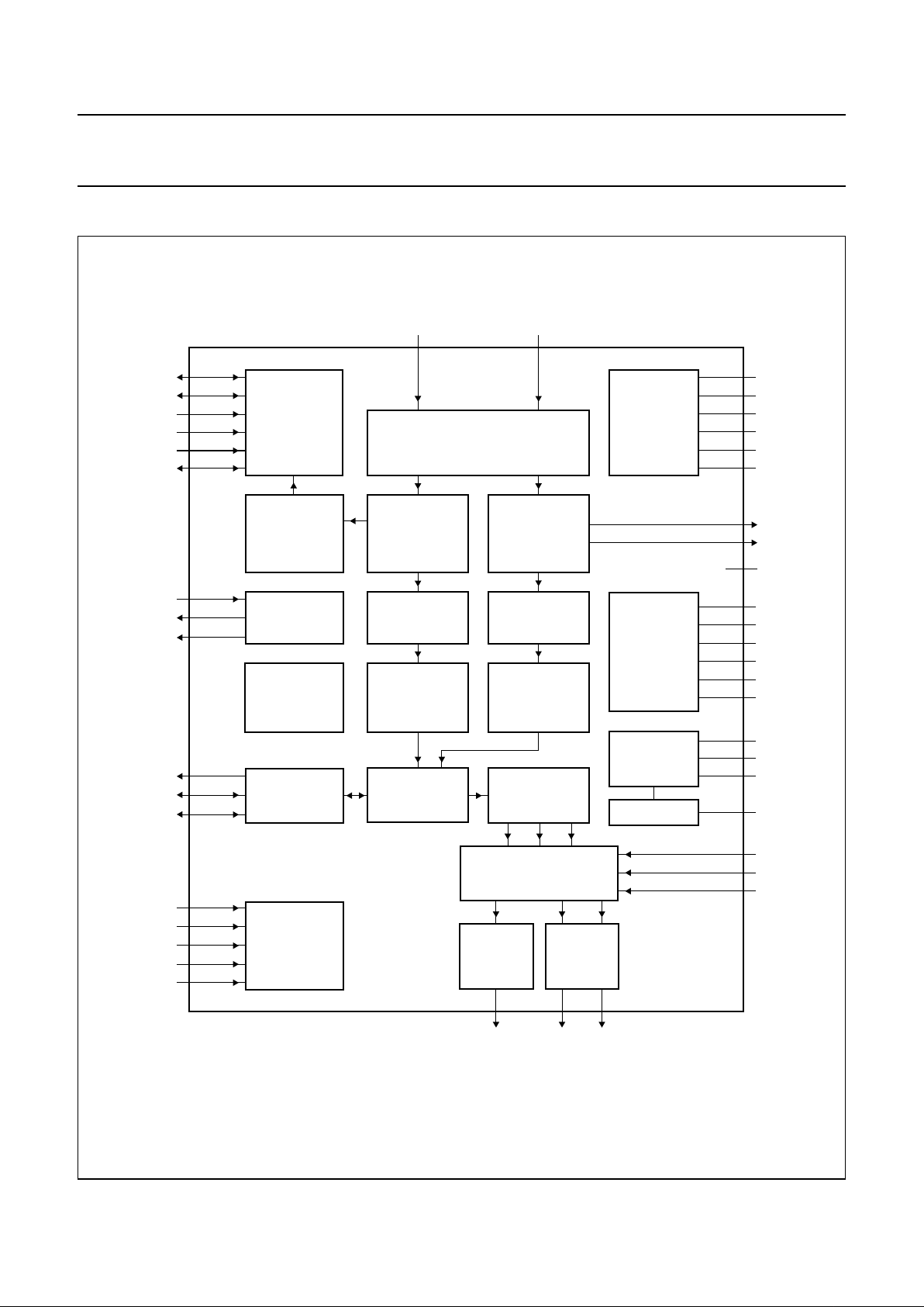
5 PINNING
SYMBOL
PIN
DESCRIPTION
SDIP42 QFP44
EXTIR 1 39 external audio input right channel
EXTIL 2 40 external audio input left channel
V
ref2
3 41 analog reference voltage for DAC and operational amplifiers
P2 4 42 second general purpose I/O pin
OUTM 5 43 analog output right
V
SSA4
6 44 analog ground supply 4 for analog back-end circuitry
OUTL 7 1 analog output left
OUTR 8 2 analog output right
V
DDA1
9 3 analog supply voltage 1; back-end circuitry 5 V
V
SSA1
10 4 analog ground supply 1; back-end circuitry
V
SSD1
11 5 digital ground supply 1; core circuitry
V
DDD1
12 6 digital supply voltage 1; core voltage regulator circuitry
V
SSD2
13 7 digital ground supply 2; core circuitry
n.c. − 8 not connected
TP2 14 9 additional test pin 2; connected to V
SSD
for normal operation
NICAM 15 10 serial NICAM data output (at 728 kHz)
TP1 16 11 additional test pin 1; connected to V
SSD
for normal operation
PCLK 17 12 NICAM clock output (at 728 kHz)
ADDR1 18 13 first I
2
C-bus slave address modifier input
XTALO 19 14 crystal oscillator output
XTALI 20 15 crystal oscillator input
TP3 − 16 additional test pin 3; connected to V
SSD
for normal operation
TEST2 21 17 test pin 2; connected to V
SSD
for normal operation
I
ref
22 18 resistor for reference current generation; front-end circuitry
ADDR2 23 19 second I
2
C-bus slave address modifier input
V
SSA2
24 20 analog ground supply 2; analog front-end circuitry
V
DEC
25 21 analog front-end circuitry supply voltage decoupling
TEST1 26 22 test pin 1; connected to V
SSD
for normal operation
SIF2 27 23 sound IF input 2
V
ref1
28 24 reference voltage; for analog front-end circuitry
SIF1 29 25 sound IF input 1
CRESET 30 26 capacitor for Power-on reset
V
SSA3
31 27 digital ground supply 3; front-end circuitry
V
DDA3
32 28 analog front-end circuitry regulator supply voltage 3 (5 V)
SCL 33 29 I
2
C-bus serial clock input
SDA 34 30 I
2
C-bus serial data input/output
SDO 35 31 I
2
S-bus serial data output
WS 36 32 I
2
S-bus word select input/output
1999 Dec 03 8
Philips Semiconductors Preliminary specification
Digital TV sound demodulator/decoder TDA9874A
SCK 37 33 I2S-bus clock input/output
SYSCLK 38 34 system clock output
V
DDD3
39 35 digital supply voltage 3; digital I/O pads
V
SSD3
40 36 digital ground supply 3; digital I/O pads
P1 41 37 first general purpose I/O pin
MONOIN 42 38 analog mono input
SYMBOL
PIN
DESCRIPTION
SDIP42 QFP44
handbook, halfpage
TDA9874APS
MHB585
1
2
42
41
3
4
5
6
7
8
9
10
11
12
13
14
15
16
17
18
19
20
40
39
38
37
36
35
34
33
32
31
30
29
28
27
26
25
24
23
2221
MONOIN
P1
V
SSD3
V
DDD3
SYSCLK
SCK
WS
SDO
SDA
SCL
V
DDA3
V
SSA3
CRESET
SIF1
V
ref1
SIF2
TEST1
V
DEC
V
SSA2
ADDR2
I
ref
EXTIR
EXTIL
V
ref2
P2
OUTM
V
SSA4
OUTL
OUTR
V
DDA1
V
SSA1
V
SSD1
V
DDD1
V
SSD2
TP2
NICAM
TP1
PCLK
ADDR1
XTALO
XTALI
TEST2
Fig.2 Pin configuration (SDIP42).
1999 Dec 03 9
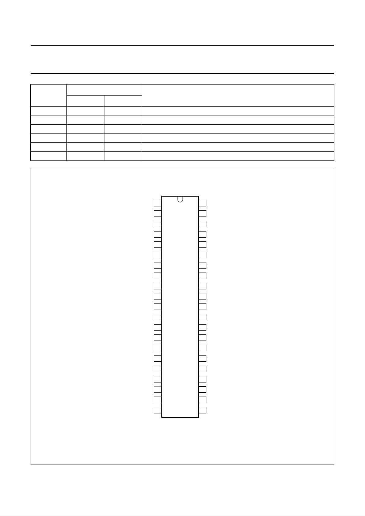
Philips Semiconductors Preliminary specification
Digital TV sound demodulator/decoder TDA9874A
handbook, full pagewidth
1
2
3
4
5
6
7
8
9
10
11
33
32
31
30
29
28
27
26
25
24
23
12
13
14
15
16
17
18
19
20
21
22
44
43
42
41
40
39
38
37
36
35
34
TDA9874AH
MHB586
SCK
WS
SDO
SDA
V
DDA3
V
SSA3
CRESET
SIF1
V
ref1
SIF2
OUTL
OUTR
V
DDA1
V
SSA1
V
SSD1
V
DDD1
n.c.
TP2
TP1
SCL
OUTM
P2
V
ref2
EXTIL
EXTIR
MONOIN
V
SSD3
V
DDD3
SYSCLK
V
SSA4
P1
ADDR1
XTALO
XTALI
TP3
TEST2
I
ref
V
SSA2
V
DEC
TEST1
PCLK
ADDR2
V
SSD2
NICAM
Fig.3 Pin configuration (QFP44).
6 FUNCTIONAL DESCRIPTION
6.1 Description of the demodulator and decoder
section
6.1.1 SIF INPUT
Two input pins are provided, SIF1 and SIF2. For higher
SIF signal levels the SIF input can be attenuated with an
internal switchable −10 dB resistor divider. As no specific
filters are integrated, both inputs have the same
specification giving flexibility in application. The selected
signal is passed through an AGC circuit and then digitized
by an 8-bit ADC operating at 24.576 MHz.
6.1.2 AGC
The gain of the AGC amplifier is controlled from the ADC
output by means of a digital control loop employing
hysteresis. The AGC has a fast attack behaviour to
prevent ADC overloads, and a slow decay behaviour to
prevent AGC oscillations. For AM demodulation the AGC
must be switched off. When switched off, the control loop
is reset and fixed gain settings can be chosen;
see Table 16.
The AGC can be controlled via the I2C-bus; details are
given in Sections 10.3.2, 10.3.3 and 10.4.6.
6.1.3 MIXER
The digitized input signal is fed to the mixers, which mix
one or both input sound carriers down to zero IF. A 24-bit
control word for each carrier sets the required frequency.
Access to the mixer control word registers is via the
I2C-bus (see Sections 10.3.5 and 10.3.6) or via Easy
StandardProgramming (ESP,seeSection 10.3.23). When
receiving NICAM programs, a feedback signal is added to
the control word of the second carrier mixer to establish a
carrier-frequency loop.
6.1.4 FM AND AM DEMODULATION
An FM or AM input signal is fed through a switchable
band-limiting filter into a demodulator that can be used for
either FM or AM demodulation. Apart from the standard
(fixed) de-emphasis characteristic, an adaptive
de-emphasis is available for Wegener-Panda 1 encoded
satellite programs.

1999 Dec 03 10
Philips Semiconductors Preliminary specification
Digital TV sound demodulator/decoder TDA9874A
6.1.5 FM DECODING
A2-carrierstereo decoder recovers the left andrightsignal
channels from the demodulated sound carriers. Both the
European and Korean stereo systems are supported.
AutomaticFMdematrixingisalso supported, which means
that the FM sound mode identification (mono, stereo or
dual) switches the FM dematrix directly. No loop via the
microcontroller is needed.
For highly overmodulated signals, a high deviation mode
for monaural audio sound single carrier demodulation can
be selected.
NICAM decoding is still possible in high deviation mode.
6.1.6 FM IDENTIFICATION
The identification of the FM sound mode is performed by
AM synchronous demodulation of the pilot and
narrow-band detection of the identification frequencies.
Theresult is available via theI2C-businterface. A selection
can be made via the I2C-bus for B/G, D/K and M
standards, and for three different time constants that
representdifferenttrade-offs between speed and reliability
ofidentification.A pilot detector allows the control software
to identify an analog 2-carrier (A2) transmission within
approximately 0.1 s.
Automatic FM dematrixing, depending on the
identification, is possible.
6.1.7 NICAM DEMODULATION
The NICAM signal is transmitted in a DQPSK code at a bit
rate of 728 kbits/s. The NICAM demodulator performs
DQPSK demodulation and passes the resulting bitstream
and clock signal to the NICAM decoder and, for evaluation
purposes, to various pins.
Atimingloop controls the frequency of thecrystaloscillator
to lock the sampling instants to the symbol timing of the
NICAM data.
6.1.8 NICAM DECODING
The device performs all decoding functions in accordance
with the
“EBU NICAM 728 specification”
. After locking to
the frame alignment word, the data is descrambled by
applying the defined pseudo-random binary sequence.
The device then synchronizes to the periodic frame flag
bit C0.
The status of the NICAM decoder can be read outfrom the
NICAM status register by the user (see Section 10.4.2).
The OSB bit indicates that the decoder has locked to the
NICAM data. The VDSP bit indicates that the decoder has
locked to the NICAM data and that the data is valid sound
data. The C4 bit indicates that the sound conveyed by the
FM mono channel is identical to the sound conveyed by
the NICAM channel.
Theerror byte contains thenumberofsound sample errors
(resulting from parity checking) that occurred in the past
128 ms period. The Bit Error Rate (BER) is approximately
0.0000174 times the contents of the error byte:
6.1.9 NICAM AUTO-MUTE
This function is enabled by setting bit AMUTE LOW
(see Section 10.3.12).Upperand lower error limits may be
definedbywriting appropriate values to two registersinthe
I2C-bussection(see Sections 10.3.14 and 10.3.15). When
thenumberoferrorsina 128 ms period exceeds the upper
error limit, the auto-mute function will switch the output
sound from NICAM to whatever sound is on the first sound
carrier (FM or AM) or to the analog mono input. When the
error count is smaller than the lower error limit, the NICAM
sound is restored.
The auto-mute function can be disabled by setting bit
AMUTE HIGH. In this case clicks become audible when
the error count increases. The user will hear a signal of
degrading quality.
If no NICAM sound is received, the outputs are switched
from the NICAM channel to the 1st sound carrier.
A decision to enable or disable the auto-mute is taken by
the microprocessor based on an interpretation of the
application control bits C1, C2, C3 and C4, and possibly
any additional strategy implemented by the user in the
microcontroller software.
When the AM sound in NICAM L systems is demodulated
in the 1st sound IF and the audio signal connected to the
mono input of the TDA9874A, the controlling
microprocessor has to ensure switching from NICAM
receptiontomonoinput,ifauto-mutingisdesired.Thiscan
be achieved by setting the AMSEL bit HIGH and the
AMUTE bit LOW (see Section 10.3.12).
BER
bit errors
total bits
-----------------------
error byte 1.74× 10
5–
×≈=
1999 Dec 03 11
Philips Semiconductors Preliminary specification
Digital TV sound demodulator/decoder TDA9874A
6.1.10 CRYSTAL OSCILLATOR
The digital controlled crystal oscillator (DCXO) is fully
integrated. Only an external 24.576 MHz crystal is
required.
6.1.11 TEST PINS
All test pins are active HIGH. In normal operation of the
device they can be left open-circuit, as they have internal
pull-down resistors. Test functions are for manufacturing
tests only and are not available to customers.
6.1.12 POWER FAIL DETECTOR
The power fail detector monitors the internal power supply
for the digital part of the device. If the supply has
temporarily been lower than the specified lower limit, the
power failure register bit PFR in subaddress 0 (see
Section 10.4.1), will be set to HIGH. The CLRPFR bit,
slave register subaddress 1 (see Section 10.3.3), resets
the Power-on reset flip-flop to LOW. If this is detected, an
initialization of the TDA9874A has to be performed to
ensure reliable operation.
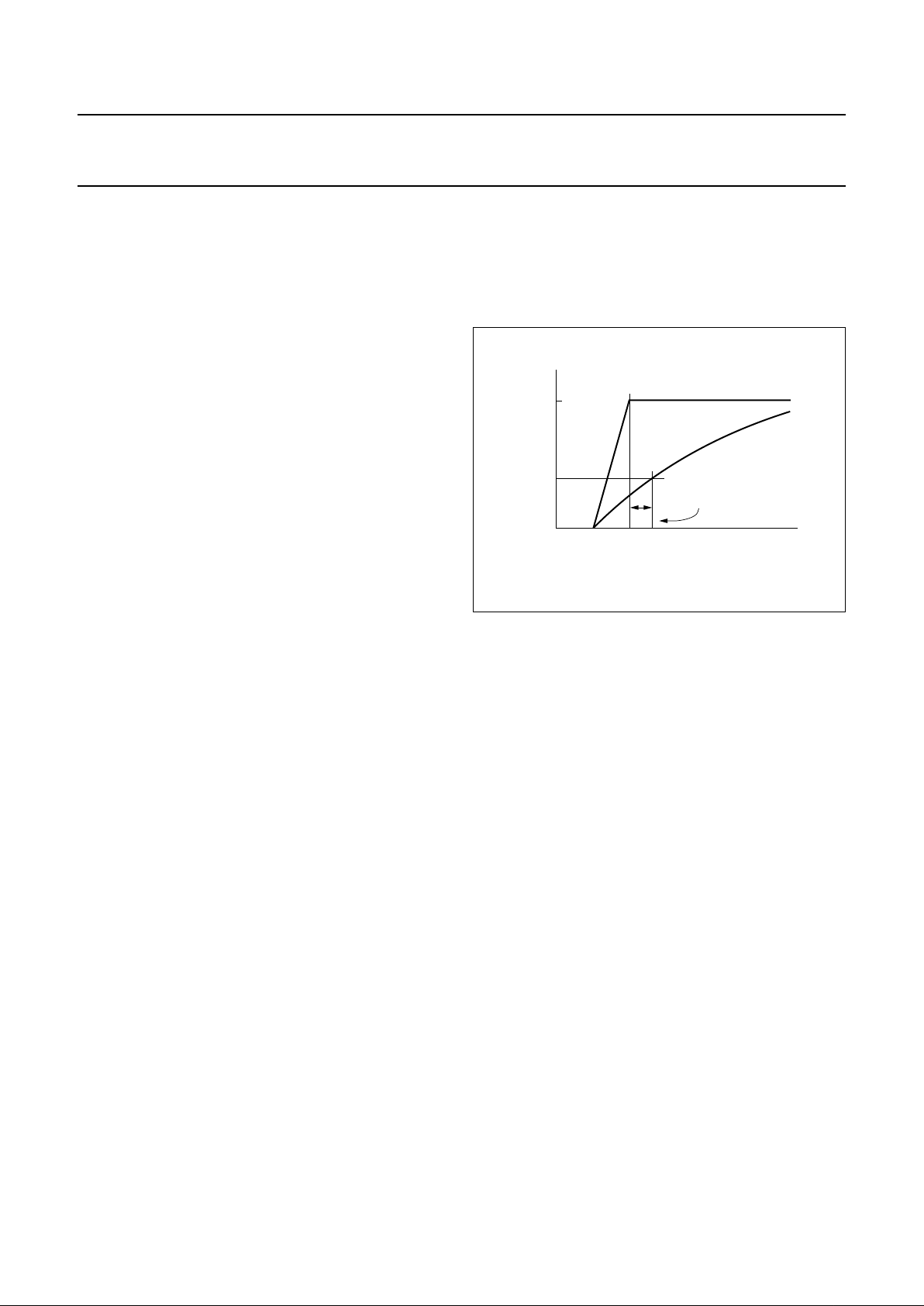
6.1.13 POWER-ON RESET
The reset is active LOW. In order to perform a reset at
power-up, a simple RC circuit may be used which consists
of an integrated passive pull-up resistor and an external
capacitor connected to ground. The pull-up resistor has a
nominal value of 50 kΩ, which can easily be measured
between pins CRESET and V
DDD3
. Before the supply
voltage has reached a certain minimum level, the state of
the circuit is completely undefined and remains in this
undefined state until a reset is applied.
The reset is guaranteed to be active when:
• The power supply is within the specified limits
(4.5 to 5.5 V)
• The crystal oscillator (DCXO) is functioning
• The voltage at pin CRESET is below 0.3V
DDD
(1.5 V if
V
DDD
= 5.0 V, typically below 1.8 V).
The required capacitor value depends on the gradient of
the rising power supply voltage. The time constant of the
RC circuit should be clearly larger than the rise time of the
power supply [to make sure that the reset condition is
always satisfied (see Fig.4)], even when considering
tolerance spreading. To avoid problems with a too slow
discharging of the capacitor at power-down, it may be
helpful to add a diode from the CRESET pin to V
DDD
.
It should be noted that the internal ESD protection diode
does not help here as it only conducts at higher voltages.
Under difficult power supply conditions (e.g. very slow or
non-monotonic ramp-up), it is recommended to drive the
reset line from a microcontroller port or the like.
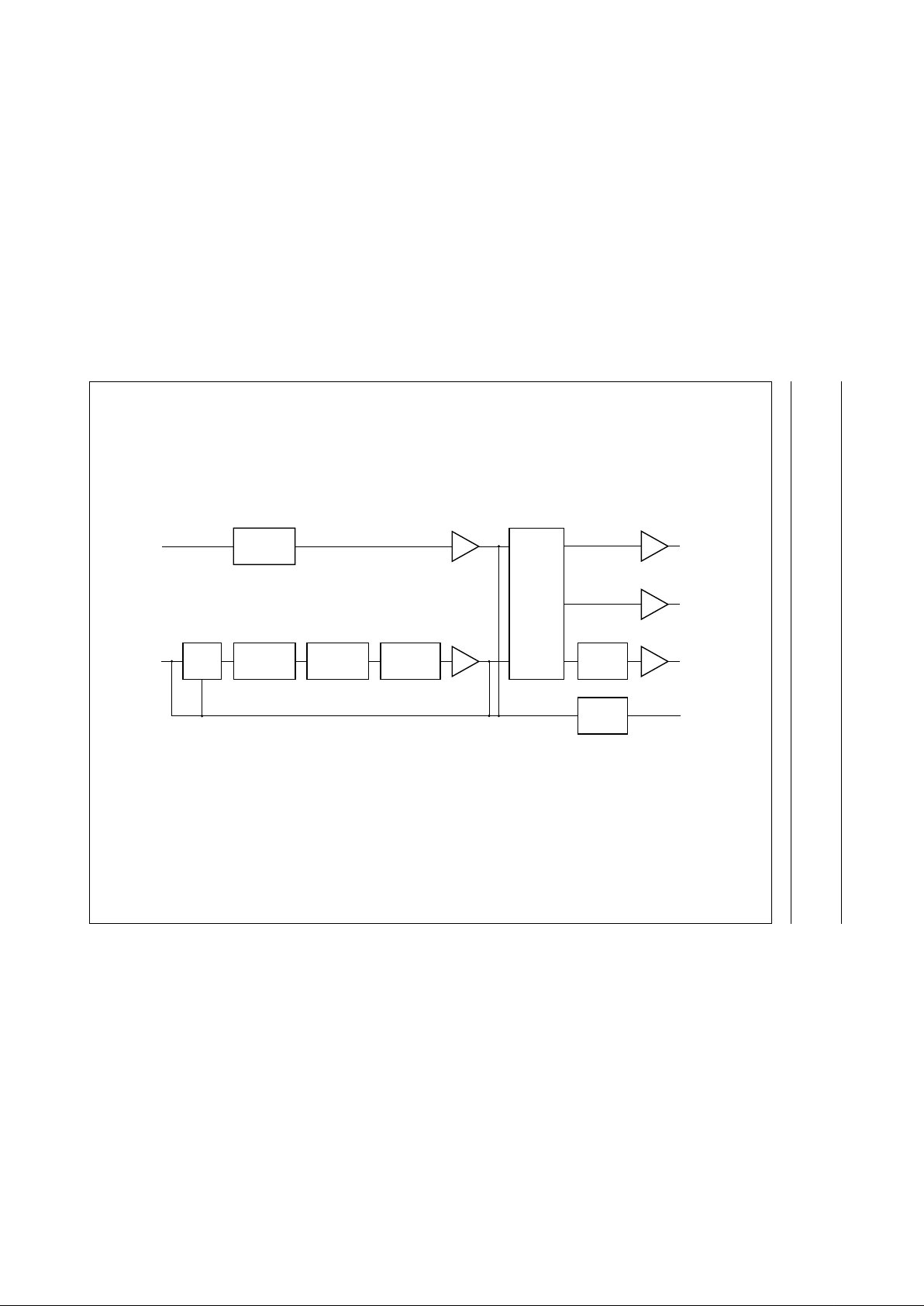
6.2 Description of the DSP
6.2.1 LEVEL SCALING
All input channels to the digital crossbar switch are
equipped with a level adjustment facility to change the
signal level in a range of ±15 dB. Adjusting the signal level
is intended to compensate for the different modulation
parameters of the various TV standards. Under nominal
conditions it is recommended to scale all input channels to
be 15 dB below full-scale [−15 dB (FS)]. This will create
sufficient headroom to cope with overmodulation and
avoids changes of the volume impression when switching
from FM to NICAM or vice versa.
6.2.2 NICAM PATH
The NICAM path has a switchable J17 de-emphasis.
6.2.3 NICAM AUTO-MUTE
If NICAM is received, the auto-mute is enabled and the
signalqualitybecomes poor. The digital crossbar switches
automatically to FM, channel 1 or the analog mono input,
as selected by bit AMSEL. This automatic switching
depends on the NICAM bit error rate. The auto-mute
function can be disabled via the I2C-bus.
handbook, halfpage
MHB587
reset active
guaranteed
1.5
5
V
t
V
CRESET
< 0.3V
DDD
V
DDD
> 4.5 V
Fig.4 Reset at power-on.

1999 Dec 03 12
Philips Semiconductors Preliminary specification
Digital TV sound demodulator/decoder TDA9874A
6.2.4 FM (AM) PATH
A high-pass filter suppresses DC offsets from the FM
demodulator that may occur due to carrier frequency
offsets, and supplies the FM monitor function with DC
values, e.g. for the purpose of microprocessor controlled
carrier search or fine tuning functions.
An adaptive de-emphasis is available for
Wegener-Panda 1 encoded satellite programs.
The de-emphasis stage offers a choice of settings for the
supported TV standards.
The 2-channel decoder performs the dematrixing of
1
⁄2(L + R), R to L and R signals of1⁄2(L + R) and1⁄2(L − R)
to L and R signals or of channel 1 and channel 2 to
L and R signals, as demanded by the different TV
standards or user preferences.
Automatic FM dematrixing is also supported.
Using the high deviation mode, only channel 1 (mono) can
be demodulated. The scaling is −6 dB compared to
2-channel decoding.
6.2.5 MONITOR
This function provides data words from the FM
demodulator outputs and FM and NICAM signals for
external use, such as carrier search or fine tuning.
The peak level of these signals can also be observed.
Source selection and data read-out are performed via the
I2C-bus.
6.2.6 DIGITAL CROSSBAR SWITCH
The input channels are derived from the FM and NICAM
paths,while the output channels comprise I2S-bus and the
audio DACs to the analog crossbar switch. It should be
noted that there is no connection from the external analog
audio inputs to the digital crossbar switch.
6.2.7 DIGITAL AUDIO OUTPUT
The digital audio output interface comprises an I2S-bus
output port and a system clock output. The I2S-bus port is
equipped with a level adjustment facility that can change
the signal level in a ±15 dB range in 1 dB steps. Muting is
possible,too, and outputs canbedisabled to improve EMC
performance.
TheI2S-busoutputmatrixprovidesthe functions for forced
mono, stereo, channel swap, channel 1 or channel 2.
Automatic selection for TV applications is possible. In this
case the microcontroller program only has to provide a
user controlled sound A or sound B selection.
6.2.8 STEREO CHANNEL TO THE ANALOG CROSSBAR PATH
A level adjustment function is provided with control
positions of 0, 3, 6 and 9 dB in combination with the audio
DACs. The Automatic Volume Level (AVL) function
provides a constant output level of −20 dB (FS) for input
levels between 0 and −26 dB (FS). There are some fixed
decay time constants to choose from, i.e. 2, 4 or 8 s.
Automatic selection for TV applications is possible. In this
case the microcontroller program only has to provide a
user controlled sound A or sound B selection.
6.2.9 GENERAL
The level adjustment functions can provide signal gain at
multiple locations. Great care has to be taken when using
gain with large input signals, e.g., due to overmodulation,
inorder not to exceed the maximum possible signal swing,
which would cause severe signal distortion. The nominal
signal level of the various signal sources to the digital
crossbar switch should be 15 dB below digital full-scale,
i.e., −15 dB (FS).
1999 Dec 03 13
Philips Semiconductors Preliminary specification
Digital TV sound demodulator/decoder TDA9874A
This text is here in white to force landscape pages to be rotated correctly when browsing through the pdf in the Acrobat reader.This text is here in
_white to force landscape pages to be rotated correctly when browsing through the pdf in the Acrobat reader.This text is here inThis text is here in
white to force landscape pages to be rotated correctly when browsing through the pdf in the Acrobat reader. white to force landscape pages to be ...
o
k, full pagewidth
MHB588
FIXED
DE-EMPHASIS
NICAM
2-CHANNEL
DECODER
FIXED
DE-EMPHASIS
ADAPTIVE
DE-EMPHASIS
DC
FILTER
FM
DIGITAL
CROSSBAR
SELECT
LEVEL
ADJUST
LEVEL
ADJUST
MONITOR
MATRIX
LEVEL
ADJUST
LEVEL
ADJUST
mono DAC
LEVEL
ADJUST
stereo DACs
I
2
S-bus
I
2
C-bus
Fig.5 DSP data flow diagram.
1999 Dec 03 14
Philips Semiconductors Preliminary specification
Digital TV sound demodulator/decoder TDA9874A
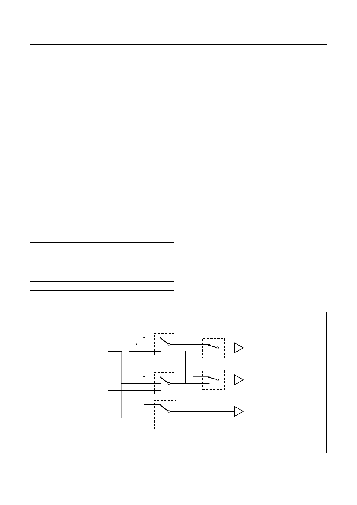
6.3 Description of the analog audio section
6.3.1 ANALOG CROSSBAR SWITCH AND ANALOG MATRIX
The TDA9874A has one external analog stereo input, one
mono input, one 2-channel and one single-channel output
port. Analog source selector switches are employed to
provide the desired analog signal routing capability, which
is done by the analog crossbar switch section.
The basic signal routing philosophy of the TDA9874A is
that each switch handles two signal channels at the same
time (e.g. left and right, language A and B) directly at the
source. For an overview of the signal flow see Fig.7.
Each source selector switch is followed by an analog
matrix to perform further selection tasks, such as putting a
signal from one input channel, say language A, to both
output channels or for swapping left and right channels.
The analog matrix provides the functions given in Table 5.
Automatic matrixing for TV applications is also supported.
All switches and matrices are controlled via the I2C-bus.
Table 5 Analog matrix functions
6.3.2 EXTERNAL AND MONO INPUTS
The external and mono inputs accept signal levels of up to
1.4 V (RMS). By adding external series resistors to
provide suitable attenuation, the external input could be
used as a SCART input. Whenever the external or mono
input is selected, the output of the DAC is muted to
improve the crosstalk performance.
6.3.3 AUDIO DACS
The TDA9874A comprises a 2-channel audio DAC and an
additional single-channel audio DAC for feeding signals
fromtheDSPsection to the analog crossbar switch. These
DACs have a resolution of 15 bits and employ four-times
oversampling and noise shaping.
6.3.4 AUDIO OUTPUT BUFFERS
The output buffers provide a gain of 0 dB and offer a
muting possibility. The post filter capacitors of the audio
DACs are connected to the buffer outputs.
6.3.5 STANDBY MODE
The standby mode (see Section 10.3.3) disables most
functions and reduces power dissipation of the
TDA9874A. It provides no other function.
Internal registers may lose their information in standby
mode. Therefore, the device needs to be initialized on
returningto normal operation. This canbeaccomplishedin
the same way as after a Power-on reset.
MODE
MATRIX OUTPUT
L OUTPUT R OUTPUT
1 L input R input
2 R input L input
3 L input L input
4 R input R input
handbook, full pagewidth
MHB589
OUTR
source select
matrix
mono (AM)
EXTIL
EXTIR
DACL
DACR
DACM
OUTL
OUTM
Fig.6 Switch diagram for the analog audio section.
1999 Dec 03 15
Philips Semiconductors Preliminary specification
Digital TV sound demodulator/decoder TDA9874A
This text is here in white to force landscape pages to be rotated correctly when browsing through the pdf in the Acrobat reader.This text is here in
_white to force landscape pages to be rotated correctly when browsing through the pdf in the Acrobat reader.This text is here inThis text is here in
white to force landscape pages to be rotated correctly when browsing through the pdf in the Acrobat reader. white to force landscape pages to be ...
handbook, full pagewidth
MHB590
2-CHANNEL
DECODER
FIXED
DE-EMPHASIS
LEVEL
ADJUST
ADAPTIVE
DE-EMPHASIS
FM/AM
DEMODULATOR
FM/AM
DE-EMPHASIS
LEVEL
ADJUST
NICAM
DECODER
NICAM
DEMODULATOR
NICAM
external
mono
DIGITAL
CROSSBAR
SELECT
LEVEL
ADJUST
AVL
MATRIX
LEVEL
ADJUST
DACs
ANALOG
CROSSBAR
SWITCH
MATRIX
BUFFER
STEREO
OUTPUT
MATRIX
BUFFER
MONO
OUTPUT
I
2
S-bus
Fig.7 Audio signal flow.

1999 Dec 03 16
Philips Semiconductors Preliminary specification
Digital TV sound demodulator/decoder TDA9874A
7 LIMITING VALUES
In accordance with the Absolute Maximum Rating System (IEC 134).
Notes
1. Human body model: C = 100 pF; R = 1.5 kΩ.
2. Machine model: C = 200 pF; L = 0.75 µH; R = 0 Ω.
8 THERMAL CHARACTERISTICS
SYMBOL PARAMETER CONDITIONS MIN. MAX. UNIT
V
DDx
DC supply voltage −0.5 +6.5 V
∆V
DDx
voltage differences between two V
DDx
pins − 550 mV
I
IK
DC input clamp diode current Vi< −0.5VorVi>VDD+ 0.5 V −±10 mA
I
OK
DC output clamp diode current output type 4 mA Vo< −0.5 V or
Vo>VDD+ 0.5 V
−±20 mA
I
O
DC output source or sink current output type
4mA
−0.5V<VO<V
DDx
+ 0.5 V −±20 mA
I
DDD
, I
SSD
DC V
DDD
or V
SSD
current per digital supply pin −±96 mA
I
DDA
, I
SSA
DC V
DDA
or V
SSA
current per analog supply pin −±50 mA
I
lu(prot)
latch-up protection current 100 − mA
P/out power dissipation per output − 100 mW
P
tot
total power dissipation − 0.75 W
T
stg
storage temperature −55 +125 °C
T
amb
ambient temperature −20 +70 °C
V
es
electrostatic handling note 1 2000 − V
note 2 200 − V
SYMBOL PARAMETER CONDITIONS VALUE UNIT
R
th(j-a)
thermal resistance from junction to ambient in free air 70 K/W

1999 Dec 03 17
Philips Semiconductors Preliminary specification
Digital TV sound demodulator/decoder TDA9874A
9 CHARACTERISTICS
VDD=5V; T
amb
=25°C; settings in accordance with B/G standard; FM deviation ±50 kHz; f
mod
= 1 kHz; FM sound
parameters in accordance with system A2; NICAM in accordance with
“EBU NICAM 728 specification”
; 1 kΩ
measurement source resistance for AF inputs; V
SIF
= 300 mV (p-p); AGCOFF = 0; AGCSLOW = 1; level and gain
settings according to note 1 with external components of Fig.9; unless otherwise specified.
SYMBOL PARAMETER CONDITIONS MIN. TYP. MAX. UNIT
Digital supplies
V
DDD1
digital supply voltage 1 4.5 5.0 5.5 V
V
SSD1
digital ground supply 1 − 0.0 − V
I
DDD1
digital supply current 1 V
DDD1
=5.5V 4059 74mA
V
DDD1
=5.0V 4259 75mA
V
SSD2
digital ground supply 2 − 0.0 − V
V
DDD3
digital supply voltage 3 4.5 5.0 5.5 V
V
SSD3
digital ground supply 3 − 0.0 − V
I
DDD3
digital supply current 3 V
DDD3
= 5.5 V; SYSCLK off 9 17 21 mA
V
DDD3
= 5.0 V; SYSCLK off 8 16 20 mA
Power failure register
V
pfr
power failure response voltage − 4.0 − V
Demodulator supplies and references
V
DDA3
analog supply voltage 3,
demodulator part
4.5 5.0 5.5 V
V
SSA3
analog ground supply 3,
demodulator part
− 0.0 − V
I
DDA3
analog supply current 3,
demodulator part
V
DDA3
=5.5V 2432 40mA
V
DDA3
=5.0V 2432 40mA
V
DEC1
analog supply decoupling
voltage for front-end
− 3.3 − V
V
SSA2
analog ground supply 2 − 0.0 − V
V
ref1
analog reference voltage,
demodulator part
− 2 − V
I
ref1(sink)
V
ref1
sink current − 200 −µA
Audio supplies and references
V
DDA1
analog supply voltage 1,
operational amplifiers
4.5 5.0 5.5 V
V
SSA1
analog ground supply 1,
operational amplifiers
− 0.0 − V
I
DDA1
analog supply current 1,
operational amplifiers
V
DDA1
= 5.5 V 3 6 10 mA
V
DDA1
= 5.0 V 3 5 10 mA
V
SSA4
analog ground supply 4, audio
DAC part
− 0.0 − V
V
ref2
referencevoltage 2,audioDACs
and operational amplifiers
referenced to V
DDA1
and
V
SSA1
− 50 − %
Z
(Vref2-VDDA3)
impedance V
ref2
to V
DDA3
− 20 − kΩ

1999 Dec 03 18
Philips Semiconductors Preliminary specification
Digital TV sound demodulator/decoder TDA9874A
Z
(Vref2-VSSA3)
impedance V
ref2
to V
SSA3
− 20 − kΩ
Digital inputs and outputs
INPUTS
CMOS level input, high drive, pull-down (pins TEST1, TEST2, TP1 and TP2)
V
IL
LOW-level input voltage −− 0.3V
DDD
V
V
IH
HIGH-level input voltage 0.7V
DDD
−−V
C
i
input capacitance −− 10 pF
Z
i
input impedance − 50 − kΩ
CMOS level input, hysteresis, high drive, pull-up (pin CRESET)
V
IL
LOW-level input voltage −− 0.3V
DDD
V
V
IH
HIGH-level input voltage 0.7V
DDD
−−V
V
hys
hysteresis voltage − 1.3 − V
C
i
input capacitance −− 10 pF
Z
i
input impedance − 50 − kΩ
INPUTS/OUTPUTS
I2C-bus level input with Schmitt trigger, open-drain output stage (pins SCL and SDA)
V
IL
LOW-level input voltage −− 0.3V
DDD
V
V
IH
HIGH-level input voltage 0.7V
DDD
−−V
V
hys
hysteresis voltage − 0.05V
DDD
− V
I
LI
input leakage current −− ±10 µA
C
i
input capacitance −− 10 pF
V
OL
LOW-level output voltage −− 0.6 V
C
L
load capacitance −− 400 pF
TTL/CMOS level, high drive, 4 mA 3-state output stage, pull-up (pins PCLK, NICAM, ADDR1, ADDR2, P1, P2, SCK,
WS and SDO)
V
IL
LOW-level input voltage −− 0.8 V
V
IH
HIGH-level input voltage 2.0 −−V
C
i
input capacitance −− 10 pF
V
OL
LOW-level output voltage IOL=3mA −− 0.4 V
V
OH
HIGH-level output voltage IOH= −3 mA 2.4 −−V
C
L
load capacitance active pull-up −− 100 pF
Z
i
input impedance − 50 − kΩ
OUTPUTS
4 mA 3-state output stage (pin SYSCLK)
V
OL
LOW-level output voltage IOL=2mA −− 0.3V
DDD
V
V
OH
HIGH-level output voltage IOH= −2 mA 0.7V
DDD
−−V
C
L
load capacitance −− 100 pF
I
LO(Z)
3-state leakage current Vi= 0 to V
DDD
−− ±10 µA
SYMBOL PARAMETER CONDITIONS MIN. TYP. MAX. UNIT

1999 Dec 03 19
Philips Semiconductors Preliminary specification
Digital TV sound demodulator/decoder TDA9874A
SIF1 and SIF2 analog inputs
V
SIF(max)(p-p)
maximum composite SIF input
voltage before clipping
(peak-to-peak value)
SIF input level adjustment
0dB
− 941 − mV
SIF input level adjustment
−10 dB
− 2976 − mV
V
SIF(min)(p-p)
minimum composite SIF input
voltage for lower limit of AGC
(peak-to-peak value)
SIF input level adjustment
0dB
− 59 − mV
SIF input level adjustment
−10 dB
− 188 − mV
AGC AGC range − 24 − dB
f
i
input frequency 4 − 9.2 MHz
R
i
input resistance AGCLEV = 0 10 −−kΩ
C
i
input capacitance − 7.5 11 pF
∆f
FM
FM deviation B/G standard; THD < 1% ±100 −−kHz
∆f
FM(FS)
FM deviation full-scale level terrestrial FM; level
adjustment 0 dB;
demodulatorfilterbandwidth
set to narrow
±150 −−kHz
∆f
FM(max)
maximum FM deviation in high
deviation mode
B/G standard; THD < 1%;
demodulatorfilterbandwidth
set to extra wide
±335 −−kHz
C/N
FM
FM carrier-to-noise ratio NFM bandwidth = 6 MHz;
white noise for S/N = 40 dB;
“CCIR468-2”
; quasi peak
− 77 −
C/N
N
NICAM carrier-to-noise ratio NN bandwidth = 6 MHz; bit
error rate = 10−3; white
noise
− 66 −
α
ct
crosstalk attenuation
SIF1 to SIF2
fi= 4 to 9.2 MHz 50 −−dB
Demodulator performance
V
o(nom)(rms)
nominal level output voltage
(RMS value)
note 1 400 500 600 mV
THD + N total harmonic distortion plus
noise
from FM source to any
output;f
i
= 1 kHz;bandwidth
20 Hz to 20 kHz;
Vo= 1 V (RMS)
− 0.3 0.5 %
from NICAM source to any
output;f
i
= 1 kHz;bandwidth
20 Hz to 20 kHz;
Vo= 1 V (RMS)
− 0.1 0.3 %
SYMBOL PARAMETER CONDITIONS MIN. TYP. MAX. UNIT
dB
Hz
------ -
dB
Hz
------ -

1999 Dec 03 20
Philips Semiconductors Preliminary specification
Digital TV sound demodulator/decoder TDA9874A
S/N signal-to-noise ratio Vo= 1 V (RMS);
“CCIR468-2”
; quasi peak
SC1 from FM source to
any output
64 70 − dB
SC2 from FM source to
any output
60 66 − dB
SC1 during use of high
deviation mode from FM
source to any output
62 68 − dB
NICAM source NICAM in accordance with
“EBU specification”
; note 2
B
(−3dB)
−3 dB bandwidth from FM source to any
output
14.5 15 − kHz
from NICAM source to any
output
14.5 15 − kHz
f
resp
frequency response
20 Hz to 14 kHz
from FM/NICAM to any
output; reference 1 kHz
−2 − +1 dB
α
cd(dual)
dual signal channel separation note3 65 70 − dB
α
cs(stereo)
stereo channel separation note 4 40 45 − dB
α
AM
AM suppression for FM AM:1 kHz, 30% modulation;
reference:fi= 1 kHz;50 kHz
deviation
50 −−dB
dm
AM
AM demodulation SIF level 100 mV (RMS);
54% AM; 1 kHz AF;
“CCIR468-2”
; quasi peak
36 45 − dB
IDENTIFICATION FOR FM SYSTEMS
m
pilot(ident)
pilot modulation for identification 25 50 75 %
C/N
pilot(ident)
pilot sideband C/N for
identification start
− 27 −
hys
(tun)
hysteresis −− 2dB
f
ident
identification window B/G stereo
slow mode 116.85 − 118.12 Hz
medium mode 116.11 − 118.89 Hz
fast mode 114.65 − 120.46 Hz
B/G dual
slow mode 273.44 − 274.81 Hz
medium mode 272.07 − 276.20 Hz
fast mode 270.73 − 277.60 Hz
t
on(ident)
total identification time on slow mode −− 2s
medium mode −− 1s
fast mode −− 0.5 s
SYMBOL PARAMETER CONDITIONS MIN. TYP. MAX. UNIT
dB
Hz
------ -

1999 Dec 03 21
Philips Semiconductors Preliminary specification
Digital TV sound demodulator/decoder TDA9874A
t
off(ident)
total identification time off slow mode −− 2s
medium mode −− 1s
fast mode −− 0.5 s
Mono and external inputs
V
i(nom)(rms)
nominal level input voltage
(RMS value)
note 1 − 500 − mV
V
i(cl)(rms)
clipping level input voltage
(RMS value)
THD < 3%; note 5 1250 1400 − mV
R
i
input resistance note 5 28 35 42 kΩ
Analog audio outputs
V
o(clip)(rms)
clipping level output voltage
(RMS value)
THD < 3% 1400 −−mV
R
o
output resistance 150 250 375 Ω
R
L(AC)
AC load resistor 10 −−kΩ
R
L(DC)
DC load resistor 10 −−kΩ
C
o(L)
output load capacitor − 10 12 nF
V
offset(DC)
static DC offset voltage − 30 70 mV
α
mute
mute suppression nominal input signal from
any source; fi= 1 kHz;
note 1
80 −−dB
B
line
bandwidth from external and mono
source; −3 dB bandwidth
20 −−kHz
G
ro
roll-off gain at 14.5 kHz from any source −3 −2 − dB
PSRR power supply ripple rejection f
ripple
= 70 Hz;
V
ripple
= 100 mV (peak);
C
Vref
=47µF; signal from
I2S-bus
40 45 − dB
Audio performance
THD + N total harmonic distortion plus
noise
V
in/out
= 1 V (RMS);
fi= 1 kHz; bandwidth
20 Hz to 20 kHz; from
external/mono input to
output copy
− 0.1 0.3 %
S/N signal-to-noise ratio reference voltage
V
0
= 1.4 V (RMS);
fi= 1 kHz;
“CCIR468-2”
;
quasi peak; from external or
mono input to output copy
78 90 − dB
α
ct
crosstalk attenuation between any analog input
pairs; fi= 1 kHz
70 −−dB
α
cs
channel separation between left and right of
external input pair
65 −−dB
between left and right of
output pair
60 −−dB
SYMBOL PARAMETER CONDITIONS MIN. TYP. MAX. UNIT
 Loading...