

Philips TDA9873HS-V1, TDA9873H-V1 Datasheet
DATA SH EET
Product specification
Supersedes data of 1999 Dec 03
File under Integrated Circuits, IC02
2000 Apr 04
INTEGRATED CIRCUITS
TDA9873H
Multistandard dual carrier stereo
sound decoder

2000 Apr 04 2
Philips Semiconductors Product specification
Multistandard dual carrier stereo sound decoder TDA9873H
FEATURES
• Low power consumption
• Alignment-free multistandard FM sound demodulation
• No externalintercarrier sound band-pass filters required
• Auto mute switchable via I2C-bus
• Multistandard A2 stereo sound decoder
• No adjustment for reduced channel separation
requirement
• De-emphasis time constant related to standard
• Very reliable digital identification of sound transmission
mode via I2C-bus, alignment-free
• No external filter for pilot input required
• I2C-bus transceiver with MAD (Module ADdress)
• I2C-bus control for all functions
• Stabilizer circuit for ripple rejection and constant output
level
• Additional mono output
• Pin aligned with TDA9874AH
• ESD protection on all pins.
GENERAL DESCRIPTION
The TDA9873H is an economic multistandard dual
FM demodulator and analog carrier stereo decoder with
I2C-bus control.
ORDERING INFORMATION
TYPE NUMBER
PACKAGE
NAME DESCRIPTION VERSION
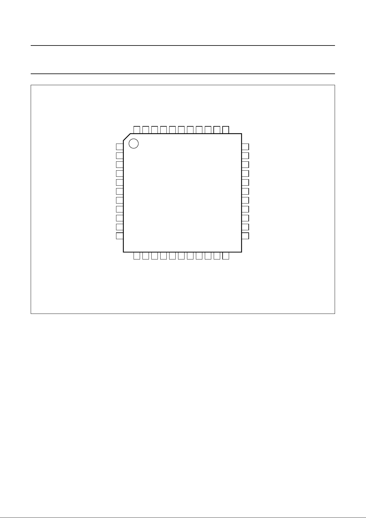
TDA9873H QFP44 plastic quad flat package; 44 leads (lead length 2.35 mm);
body 14 × 14 × 2.2 mm
SOT205-1
TDA9873HS QFP44 plastic quad flat package; 44 leads (lead length 1.3 mm);
body 10 × 10 × 1.75 mm
SOT307-2
2000 Apr 04 3
Philips Semiconductors Product specification
Multistandard dual carrier stereo sound decoder TDA9873H
QUICK REFERENCE DATA
VCC=5V; T
amb
=25°C; B/G standard (f
SC1
= 5.5 MHz, f
SC2
= 5.742 MHz, SC1/SC2=7dB,∆fAF= 27 kHz,
f
mod
= 1 kHz, L = R, stereo mode); input level for first sound carrier V
i(FM)(rms)
=50mV; f
ref
= 4.000 MHz; measured in
application circuits of Figs 7 and 8; unless otherwise specified.
Notes
1. Condition for B/G, I and D/K standard: V
CC
= 5 V and ∆f = 27 kHz (m = 54%). Condition for M standard: VCC=5V
and ∆f = 13.5 kHz; 6 dB gain added internally to compensate smaller deviation.
2. The maximum total system identification time ‘on’ for a channel change is equal to maximum value of t
ident(on)
plus
t
I2C(read-out)
. The maximum total system identification time ‘off’ for a channel change is equal to maximum value of
t
ident(off)
plus t
I2C(read-out)
. The fast mode is proposed mainly during search tuning, program or channel select. If the
channel is selected, the identification response should be switched to normal mode for improved reliability. However
due to the transition from fast to normal mode, the identification bits are not valid for one integrator period. Therefore
the transmitter mode detected during the fast mode has to be stored before changing to normal mode. The storage
has to be kept for two seconds (maximum value of t
ident(on)
in the normal mode) from the moment of transition.
The identification can now operate in the normal mode until the next tuning action.
3. R modulated and L monitored.
SYMBOL PARAMETER CONDITIONS MIN. TYP. MAX. UNIT
V
CC
supply voltage 4.5 5 6.6 V
I
CC
supply current 40 60 75 mA
V
o(rms)
AF output level (RMS value) 54% modulation; note 1 400 500 600 mV
V
o(cl)(rms)
AF output clipping level
(RMS value)
THD < 1.5% 1400 −−mV
f
i(FM)
FM-PLL operating frequencies
(switchable)
first sound carrier
M standard − 4.5 − MHz
B/G standard − 5.5 − MHz
I standard − 6.0 − MHz
D/K standard − 6.5 − MHz
second sound carrier
M standard − 4.72 − MHz
B/G standard − 5.74 − MHz
D/K (1) standard − 6.26 − MHz
D/K (2) standard − 6.74 − MHz
D/K (3) standard − 5.74 − MHz
S/N
W
weighted signal-to-noise ratio
(complete signal path)
CCIR 468-4 weighted; quasi
peak; dual mode;
B/G standard; note 1
52 56 − dB
t
ident(on)
total identification time on for
identification mode change
normal mode; note 2 0.35 − 2s
fast mode; note 2 0.1 − 0.5 s
V
i(FM)(rms)
FM-PLL input voltage (RMS value) sensitivity for pull-in
first sound carrier −−6mV
second sound carrier −−1mV
α
cs(AF)(stereo)
AF channel separation (stereo
mode; complete signal path)
B/G standard; note 3
without alignment 25 30 − dB
I2C-bus alignment 40 45 − dB
α
ct(AF)(dual)
AF crosstalk attenuation (dual
mode; complete signal path)
65 70 − dB
2000 Apr 04 4
Philips Semiconductors Product specification
Multistandard dual carrier stereo sound decoder TDA9873H
This text is here in white to force landscape pages to be rotated correctly when browsing through the pdf in the Acrobat reader.This text is here in
_white to force landscape pages toberotated correctly when browsing through the pdf in the Acrobat reader.This text is here inThis text is here in
white to force landscape pages to be rotated correctly when browsing through the pdf in the Acrobat reader. white to force landscape pages to be ...
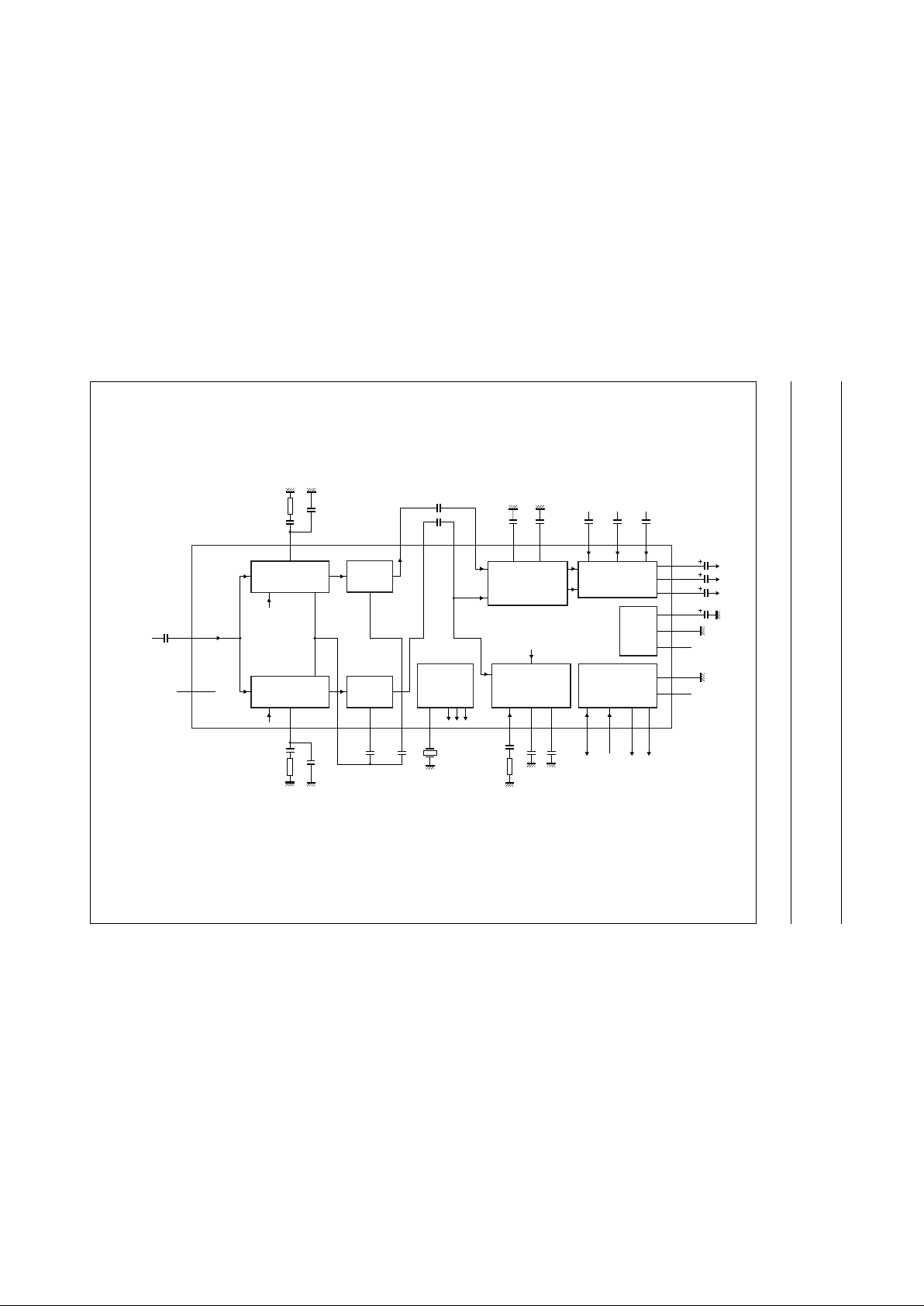
BLOCK DIAGRAM
n
dbook, full pagewidth
MHB429
FM DEMODULATOR
NARROW-BAND PLL
SC2
FM DEMODULATOR
NARROW-BAND PLL
SC1
AF
AMPLIFIER
2
AF
AMPLIFIER
1
LF2
18
4, 5, 9, 11, 12,
16, 17, 19, 20,
22, 23, 36, 44
LPF31CID35CTRIG
34
25
AFR13CAF2
26
DIGITAL
ACQUISITION
OSCILLATOR
CLOCK
STEREO DECODER
STEREO ADJUST
B/G, D/K, I, M (Korea)
STANDARD
AF SWITCH
DIGITAL
IDENTIFICATION
PILOT
NARROW-BAND PLL
SDA30SCL29P137P2
42
I
2
C-BUS
TRANSCEIVER
XTAL
4 MHz
15
CAF1
24
TDA9873H
loop filter
14
LF1
3
CDE16CDE2
38
EXTM
M
39
EXTR
R
mono stereo
40
EXTL
L
8
AF1IAF2I
321033
AF1O AF2O
loop filter
IFINT
n.c.
DGND27
MAD21
POWER
SUPPLY
AGND
OUTM
7
V
CC
V
ref
28
41
43
IF
intercarrier
input
4.5, 5.5, 6.0, 6.5
4.72, 5.74, 6.26,
6.74 MHz
pilot
loop
external AF
OUTR
2
OUTL
1
Fig.1 Block diagram.
2000 Apr 04 5
Philips Semiconductors Product specification
Multistandard dual carrier stereo sound decoder TDA9873H
PINNING
SYMBOL PIN DESCRIPTION
OUTL 1 left audio output
OUTR 2 right audio output
CDE1 3 de-emphasis 1 capacitor
n.c. 4 not connected
n.c. 5 not connected
CDE2 6 de-emphasis 2 capacitor
AGND 7 analog ground
AF1I 8 audio 1 input
n.c. 9 not connected
AF1O 10 audio 1 output
n.c. 11 not connected
n.c. 12 not connected
AFR 13 AF1 and AF2 signal return
LF1 14 loop filter 1
XTAL 15 4 MHz reference input
n.c. 16 not connected
n.c. 17 not connected
LF2 18 loop filter 2
n.c. 19 not connected
n.c. 20 not connected
MAD 21 programmable address bit
(module address)
n.c. 22 not connected
n.c. 23 not connected
CAF1 24 audio 1 (AF1) capacitor
IFINT 25 IF intercarrier input
CAF2 26 audio 2 (AF2) capacitor
DGND 27 digital ground
V
CC
28 supply voltage (+5 V)
SCL 29 serial clock input (I
2
C-bus)
SDA 30 serial data input/output (I
2
C-bus)
LPF 31 pilot loop filter
AF2O 32 audio 2 output
AF2I 33 audio 2 input
CTRIG 34 trigger capacitor
CID 35 identification capacitor
n.c. 36 not connected
P1 37 output port 1
EXTM 38 external audio input mono
EXTR 39 external audio input right
EXTL 40 external audio input left
V
ref
41 reference voltage (1⁄2VCC)
P2 42 output port 2
OUTM 43 mono output
n.c. 44 not connected
SYMBOL PIN DESCRIPTION
2000 Apr 04 6
Philips Semiconductors Product specification
Multistandard dual carrier stereo sound decoder TDA9873H
Fig.2 Pin configuration.
handbook, full pagewidth
1
2
3
4
5
6
7
8
9
10
11
33
32
31
30
29
28
27
26
25
24
23
12
13
14
15
16
17
18
19
20
21
22
44
43
42
41
40
39
38
37
36
35
34
TDA9873H
MHB430
AF2I
AF2O
LPF
SDA
V
CC
DGND
CAF2
IFINT
CAF1
n.c.
OUTL
OUTR
CDE1
n.c.
n.c.
CDE2
AF1I
n.c.
n.c.
SCL
OUTM
P2
V
ref
EXTL
EXTR
EXTM
n.c.
CID
CTRIG
n.c.
P1
AFR
LF1
XTALI
n.c.
n.c.
LF2
n.c.
MAD
n.c.
n.c.
n.c.
AGND
AF1O

2000 Apr 04 7
Philips Semiconductors Product specification
Multistandard dual carrier stereo sound decoder TDA9873H
FUNCTIONAL DESCRIPTION
FM demodulators
The FM demodulators are Narrow-Band Phase-Locked
Loops (NBPLLs) with external loop filters, to provide the
required selectivity. To achieve good selectivity, linear
Phase Detectors (PDs) and constant input levels are
required. The intercarrier signal from the input terminal is
fed via high-pass filters and gain controlled amplifiers to
the phase detectors. A carrier cancellation circuit placed
before the amplifier for the second PLL is used to reduce
the first sound carrier. The PD output signals control the
integrated relaxation oscillators via the loop filters.
The frequency range is approximately 4 to 7 MHz. As a
result of locking, the oscillator frequency tracks with the
modulation of the input signal and the oscillator control
voltages are superimposed by the AF voltages. Using this
method, the FM-PLLs operate as FM demodulators.
The AF voltages are present at the loop filters and fed via
buffers with 0 dB gain to the audio amplifiers.
The supported standards and their characteristics are
given in Table 1.
Digital acquisition help
A narrow-band PLL requires a measure to lock to the
wanted input signal. Each relaxation oscillator of the three
integrated PLLs (first and second sound carriers and pilot
carrier) has a wide frequency range. To guarantee correct
locking of the PLL with respect to the catching range, the
digital acquisition help provides individual control until the
VCO frequency is within the standard and PLL dependent
lock-inwindow, related tothestandard dependent carriers.
It ensures that the oscillator frequency of the FM-PLL is
within ±225 kHz of the sound carrier to be demodulated.
The pilot carrier frequency window is ±150 Hz.
The working principal of the digital acquisition help is as
follows. The VCOs are connected, one at a time, to a
down-counter. The counter start value is standard
dependent and predefined for each of the three PLLs.
After a given counting time the stop value of the
down-counter is probed.
If the stop value is lower (higher) than the expected value
range,the VCO frequency is higher (lower)thanthelock-in
window. A negative (positive) control current is injected
into the loop filter for a short time, thereby decreasing
(increasing) the VCO frequency by a proportional value.
Ifthe stop value meets the expected value range, the VCO
frequency is within the defined lock-in window and no
control current is injected into the loop filter.
In an endless circle the VCO of the next PLL will be
connected to the down-counter and the described
procedure starts again.
The whole tracing as well as the counting time itself is
derived from the external frequency reference. The cycle
time is 256 µs.
Auto mute
If a sound carrier is missed, acquisition pulses are
generated when the NBPLL frequency leaves the window
edges. To avoid noise at the audio output, an I2C-bus
switchable mute-enable stage is built in. If auto mute is
enabled via the I2C-bus, the circuit mutes immediately
after the first acquisition pulse. If a sound carrier occurs
(no further acquisition pulses), the mute stage
automatically returns to active mode after 40 ms.
If the first sound carrier is not present, the second audio
channel will also be muted.
Audio preamplifier
The AF preamplifiers are operational amplifiers with
internal feedback, high gain and high common mode
rejection. The AF voltages from the PLL demodulators
(small output signals) are amplified by approximately
34 dB. Using a DC operating point control circuit, the
AF amplifiers are decoupled from the PLL DC voltage.
The amplified AF signals are available at the output
terminals and fed via external decoupling capacitors to the
stereo decoder input terminals.
Stereo decoder
The input circuit incorporates a soft-mute stage which is
controlled by the FM-PLL acquisition circuit. The auto
mute function can be disabled via the I2C-bus.
The AF output voltage is 500 mV (RMS) for 54%
modulation, clipping therefore may occur at high
over-modulation. If more headroom is required the input
signal can be attenuated by 6 dB via the I2C-bus.
A stereo adjustment (see Fig.6) is incorporated to correct
theFM demodulator outputvoltage spread(see Table 19).
If no I2C-bus adjustment is required (potentiometer
adjustment or no adjustment) the default value should be
0 dB for B/G, M and D/K (2) standard. For the standards
D/K (1) and D/K (3) the second sound carrier frequency is
below the first sound carrier which results in a lower
AF output level for the second sound carrier. In this state,
a gain of +0.1 dB for D/K (1) and +0.2 dB for D/K (3) is
preferred.

2000 Apr 04 8
Philips Semiconductors Product specification
Multistandard dual carrier stereo sound decoder TDA9873H
In the following dematrix, the modes stereo, mono and
dual are processed for the different standards. The 6 dB
level difference between B/G and M standard is
automatically compensated in the dematrix, therefore no
further level adaption is needed.
De-emphasis is performed by two RC low-pass filter
networks with internal resistors and external capacitors.
The time constant is automatically switched to 50 µs or
75 µs according to the chosen standard.
Due to some frequency response peaking of the
FM demodulation, compensation is necessary. This is
done by having a slightly larger time constant for the
de-emphasis.
All other settings such as AF switch, stereo channel
adjustment values or default corrections have to be
controlled via the I2C-bus depending on the identification
or user definition.
AF switch
The circuit incorporates a single stereo and mono
AF output. Using rail-to-rail operational amplifiers, the
clipping level is set to 1.4 V (RMS) for VCC=5V.
As well as the internal stereo decoder output signal, one
externalstereo and one mono input can be switched to the
AF outputs. Both the mono and stereo outputs can be
switched independent of the internal or external sources
(see Tables 13 and 25). Fig.6 shows the switch
configurations.
A nominal gain of 0 dB for the signals from the external
inputs to the outputs is built-in.
Stereo/dual sound identification
The pilot signal is fed to the input of a NBPLL. The PLL
circuitgenerates the synchronizedpilotcarrier. This carrier
is used for the synchronous AM demodulation to get the
low-pass filtered identification signal.
A Schmitt trigger circuit performs pulse shaping of the
identificationsignalwhenthesignallevel is higher than the
Schmitt trigger threshold. For smaller signal levels there is
no AC output signal, thus protecting against
mis-identification caused by spurious signal components.
The identification stages consist of two digital PLL circuits
anddigitalintegratorstogeneratethestereo or dual sound
identification bits, which can be read out via the I2C-bus.
A 4 MHz crystal oscillator provides the reference clock
frequency. The corresponding detection bandwidth is
larger than ±50 Hz for the pilot carrier signal, so that
f
pilot
variations from the transmitter can be tracked in the
event of missing synchronization with the horizontal
frequency fH. However, the detection bandwidth for the
identification signal is limited to approximately ±1 Hz for
high identification reliability.
I
2
C-bus transceiver
The TDA9873H is microcontroller controlled via a 2-wire
I2C-bus.
Two wires, serial data (SDA) and serial clock (SCL) carry
information between the devices connected to the bus.
The TDA9873H has an I2C-bus slave transceiver with
auto-increment.
To avoid conflicts in applications with other ICs providing
similar or complementary functions, two slave addresses
are available, selected on the pin MAD. A slave address is
sent from the master to the slave receiver.
In the TV sound processor family several devices are
available. To identify the TDA9873H device, the master
sends a slave address with R/W bit = 0. The slave then
generates an acknowledge and the master sends the data
subaddress 254 to the slave, followed by an acknowledge
from the slave to the master. The master then sends the
slave address with R/W bit = 1. The slave then transmits
the device identification code 80H to the master, followed
by an acknowledge NOT and a STOP condition generated
by the master.
Control ports
Two digital open-collector output ports P1 and P2 provide
external switching functions in the receiver front-end or
IF demodulators. The ports are controlled by the I2C-bus
(see Tables 22 and 23) and are freely programmable.
2000 Apr 04 9
Philips Semiconductors Product specification
Multistandard dual carrier stereo sound decoder TDA9873H
Power supply
The different supply voltages and currents required for the
analog and digital circuits are derived from two internal
band gap reference circuits. One of the band gap circuits
internally generates a voltage of approximately 2.4 V,
independent of the supply voltage and temperature.
A voltage regulator circuit, connected to this voltage,
produces a constant voltage of 3.55 V which is used as an
internalreference voltage. The AF referencevoltageV
ref
is
1
⁄2VCC. Good ripple rejection is achieved with the external
capacitor C
ref
=47µF (16 V) in combination with an
internal resistor at pin 6. No additional DC load for1⁄2V
CC
is allowed.
Analog ground (AGND, pin 7) and digital ground
(DGND, pin 27) should be connected directly to the IC.
Pin 13 is internal analog ground.
Power-on reset
When a Power-on reset is activated by switching on the
supply voltage or because of a supply voltage breakdown,
the 117/274 Hz DPLL, 117/274 Hz integrator and the
registers will be reset. Both AF channels (main and mono)
are muted. The ports are in position HIGH. Gain stereo
adjustment is 0 dB. Auto mute is active. For detailed
information see Table 12.
LIMITING VALUES
In accordance with the Absolute Maximum Rating System (IEC 60134).
Notes
1. I
CC
= 60 mA; T
amb
=70°C.
2. Machine model class B: C = 200 pF; L = 0.75 µH; R = 0 Ω.
3. Human body model class B: C = 100 pF; R = 1.5 kΩ.
THERMAL CHARACTERISTICS
SYMBOL PARAMETER CONDITIONS MIN. MAX. UNIT
V
CC
supply voltage (pin 28) maximum chip
temperature of 125 °C;
note 1
0 6.8 V
V
i
input voltage at:
pins 1 to 6, 8 to 12, 14 to 26 and 31 to 44 0 V
CC
V
pins 29 to 30 −0.3 V
CC
V
T
stg
storage temperature −25 +150 °C
T
amb
ambient temperature −20 +70 °C
V
es
electrostatic handling voltage note 2 −150 +150 V
note 3 −2500 +2500 V
SYMBOL PARAMETER CONDITIONS VALUE UNIT
R
th(j-a)
thermal resistance from junction to ambient in free air
TDA9873H 70 K/W
TDA9873HS 65 K/W

2000 Apr 04 10
Philips Semiconductors Product specification
Multistandard dual carrier stereo sound decoder TDA9873H
CHARACTERISTICS
VCC=5V; T
amb
=25°C; B/G standard (f
SC1
= 5.5 MHz, f
SC2
= 5.742 MHz, SC1/SC2=7dB,∆fAF= 27 kHz,
f
mod
= 1 kHz, L = R, stereo mode); input level for first sound carrier V
i(FM)(rms)
=50mV; f
ref
= 4.000 MHz; measured in
application circuits of Figs 7 and 8; unless otherwise specified.
SYMBOL PARAMETER CONDITIONS MIN. TYP. MAX. UNIT
Supply (pin 28)
V
CC
supply voltage 4.5 5 6.6 V
I
CC
supply current 40 60 75 mA
FM-PLL demodulator (pin 25); note 1
V
i(FM)(rms)
FM-PLL input voltage
(RMS value)
sensitivity for pull-in
first sound carrier −−6mV
second sound carrier −−1mV
level for gain controlled
operation; note 2
first sound carrier 6 − 150 mV
second sound carrier 1 − 100 mV
V
i(vid)(p-p)
allowable interference video
level (peak-to-peak value)
see Fig.3
V
i(FM1)(rms)
=6mV −−160 mV
V
i(FM1)(rms)
= 150 mV −−2V
R
i
input resistance 4 5 6 kΩ
f
i(FM)
FM-PLLoperatingfrequencies
(switchable)
first sound carrier
M standard − 4.5 − MHz
B/G standard − 5.5 − MHz
I standard − 6.0 − MHz
D/K standard − 6.5 − MHz
second sound carrier
M standard − 4.72 − MHz
B/G standard − 5.74 − MHz
D/K (1) standard − 6.26 − MHz
D/K (2) standard − 6.74 − MHz
D/K (3) standard − 5.74 − MHz
∆f
FM
frequency windows of digital
acquisition help
narrow; note 3 −±225 − kHz
wide; note 3 −±450 − kHz
∆f
AF
frequency deviation THD < 1.5%; normal gain −−±62 kHz
THD < 1.5%; reduced gain −−±124 kHz
∆f
AF(ident)
frequency deviation for safe
identification
VCC= 5 V; stereo: 1 kHz L,
400 Hz R
−−±125 kHz
α
AM
AM suppression AM: f
mod
= 1 kHz; m = 0.3
referenced to 27 kHz
FM deviation
40 46 − dB
K
O(FM)
VCO steepness ∆fFM/∆V
LF1,2
note 4 − 3.3 − MHz/V
K
D(FM)
phase detector steepness
∆I
LF1,2
/∆ϕ(VFM)
note 4 − 4 −µA/rad

2000 Apr 04 11
Philips Semiconductors Product specification
Multistandard dual carrier stereo sound decoder TDA9873H
V
CAF
DC voltage at CAF1 and
CAF2
dependent on intercarrier
frequency f
FM
0.6 − 2.6 V
B
AF(−3dB)
−3 dB audio frequency
bandwidth
measured at AF1O and
AF2O; see Figs 7 and 8
upper limit dependent on
loop filter; note 4
65 80 − kHz
lower limit dependent on
CAF;CAF= 470 nF; note 5
−−20 Hz
V
o(FM)(rms)
output level (RMS value) measured at
AF1O and AF2O
− 250 − mV
Audio processing (pins 1, 2, 8 and 33)
V
o(rms)
AF output level (RMS value) f
mod
= 300 Hz;
54% modulation;
switchable by I2C-bus;
note 6
normal gain 400 500 600 mV
reduced gain 200 250 300 mV
V
o(cl)(rms)
AF output clipping level
(RMS value)
VCC= 5 V; THD = 1.5% 1400 −− mV
R
L
allowable load resistance AC coupled 10 −− kΩ
C
L
allowable load capacitance −−1.5 nF
R
L(DC)
allowable DC load resistance 100 −− kΩ
R
o
output resistance 70 150 300 Ω
THD total harmonic distortion V
o(rms)
= 0.5 V; fAF= 1 kHz − 0.2 0.5 %
α
cs(AF)(stereo)
AF channelseparation (stereo
mode; complete signal path)
without alignment; note 7
B/G or M (Korea)
standard
25 30 − dB
D/K standard 23 27 − dB
potentiometer alignment;
B/G, M and D/K standard;
notes 7 and 8
35 40 − dB
I2C-bus alignment;
notes 7 and 9
B/G and D/K standard 40 45 − dB
M standard 35 40 − dB
α
ct(AF)(dual)
AF crosstalk attenuation (dual
mode)
fi= 1 kHz for signal A;
fi= 400 Hz for signal B;
∆f=±50 kHz
complete signal path 65 70 − dB
stereo decoder only 70 75 − dB
α
mute(AF)
mute attenuation of AF signal 75 80 − dB
SYMBOL PARAMETER CONDITIONS MIN. TYP. MAX. UNIT
2000 Apr 04 12
Philips Semiconductors Product specification
Multistandard dual carrier stereo sound decoder TDA9873H
S/N
W
weighted signal-to-noise ratio
(complete signal path)
CCIR 468-4 weighted;
quasi peak; dual mode;
note 6
50 µs de-emphasis;
B/G, I and D/K standard
52 56 − dB
75 µs de-emphasis;
M standard
48 52 − dB
S/N
W(d)
signal-to-noise ratio at
external AF with stereo
decoder only
CCIR 468-4 weighted;
quasi peak;
V
o(rms)
= 500 mV
70 75 − dB
t
DEP(B/G)
de-emphasis time constant for
B/G, D/K and I standard
note 10; see Fig.4 − 50 −µs
t
DEP(M)
de-emphasis time constant for
M standard
note 10; see Fig.4 − 75 −µs
f
ro
roll-off frequency 470 nF at AF1I and AF2I;
without de-emphasis
low frequency (−3 dB) −−20 Hz
high frequency (−0.5 dB) 20 −− kHz
PSRR power supply ripple rejection
at OUTL and OUTR (overall
performance)
f
ripple
= 70 Hz;
V
ripple(p-p)
= 100 mV;
dual mode; see Fig.5
20 26 − dB
R
i(AF1)
AF1I input resistance 32 40 48 kΩ
R
i(AF2)
AF2I input resistance 32 40 48 kΩ
External additional inputs (pins 38 to 40)
V
i(nom)(rms)
nominal input signal voltage
(RMS value)
− 0.5 − V
V
i(cl)(rms)
clipping voltage level
(RMS value)
THD ≤ 1.5%; VCC= 5 V 1.4 −− V
G
v
AF signal voltage gain G = Vo/V
i
−1 0 +1 dB
R
i
input resistance 40 50 60 kΩ
f
ro
roll-off frequency low frequency (−3 dB) −−20 Hz
high frequency (−0.5 dB) 20 −− kHz
α
ct(ext)
AF crosstalk attenuation
(external input)
f
i(EXTL)
= 1 kHz;
f
i(EXTR)
= 400 Hz
70 75 − dB
Mono output OUTM (pin 43)
R
o
output resistance 70 200 350 Ω
R
L
load resistance AC coupled 10 −− kΩ
R
L(DC)
allowable DC load resistance 100 −− kΩ
C
L
load capacitance −−1.5 nF
α
mute
mute attenuation 60 −− dB
SYMBOL PARAMETER CONDITIONS MIN. TYP. MAX. UNIT
 Loading...