

Philips TDA9861 Datasheet

INTEGRATED CIRCUITS
DATA SH EET
TDA9861
Universal HiFi audio processor for
TV
Preliminary specification
File under Integrated Circuits, IC02
June 1994
Philips Semiconductors Preliminary specification
Universal HiFi audio processor for TV TDA9861
FEATURES
• Multi-source selector switches six AF inputs (three
stereo sources or six mono sources)
• Each of the input signals can be switched to each of the
outputs (crossbar switch)
• Outputs for loudspeaker channel, headphone channel
and peri-TV connector (SCART)
• Switchable spatial stereo and pseudo stereo effects
• Audio surround decoder can be added externally
• Two general purpose logic output ports
• I2C-bus control of all functions.
QUICK REFERENCE DATA
SYMBOL PARAMETER MIN. TYP. MAX. UNIT
V
P
I
P
V
i
positive supply voltage (pin 6) 7.2 8.0 8.8 V
supply current − 25 − mA
input signal levels for 0 dB gain
(RMS value)
V
o
output signal levels for 0 dB
gain (RMS value)
G
v
gain in main channel
volume control (1 dB steps,
balance included)
bass control (1.5 dB steps) −12 − +15 dB
treble control (3 dB steps) −12 − +12 dB
gain in headphone channel
volume control (2 dB steps) −54 − +16 dB
gain for muting in all channels −80 −−dB
THD total harmonic distortion − 0.1 − %
S/N signal-to-noise ratio − 85 − dB
T
amb
operating ambient temperature 0 − +70 °C
GENERAL DESCRIPTION
The TDA9861 provides control facilities for the main, the
headphone and the SCART channel of a TV set. Due to
extended switching possibilities, signals from 3 stereo
sources can be handled.
2 −−V
2 −−V
−63 − +15 dB
ORDERING INFORMATION
EXTENDED TYPE
NUMBER
PINS PIN POSITION MATERIAL CODE
TDA9861 32 SDIL plastic SOT232
Note
1. SOT232-1; 1996 December 10.
June 1994 2
PACKAGE
(1)
Philips Semiconductors Preliminary specification
Universal HiFi audio processor for TV TDA9861
June 1994 3
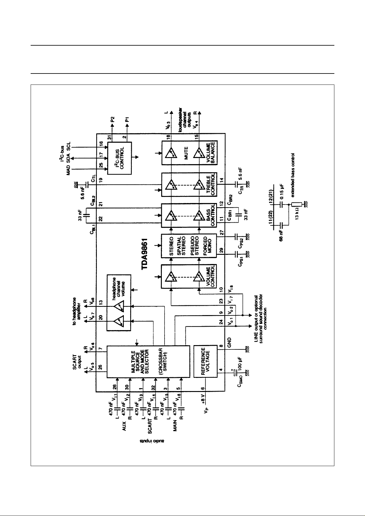
Fig.1 Block diagram and application circuit.
Philips Semiconductors Preliminary specification
Universal HiFi audio processor for TV TDA9861
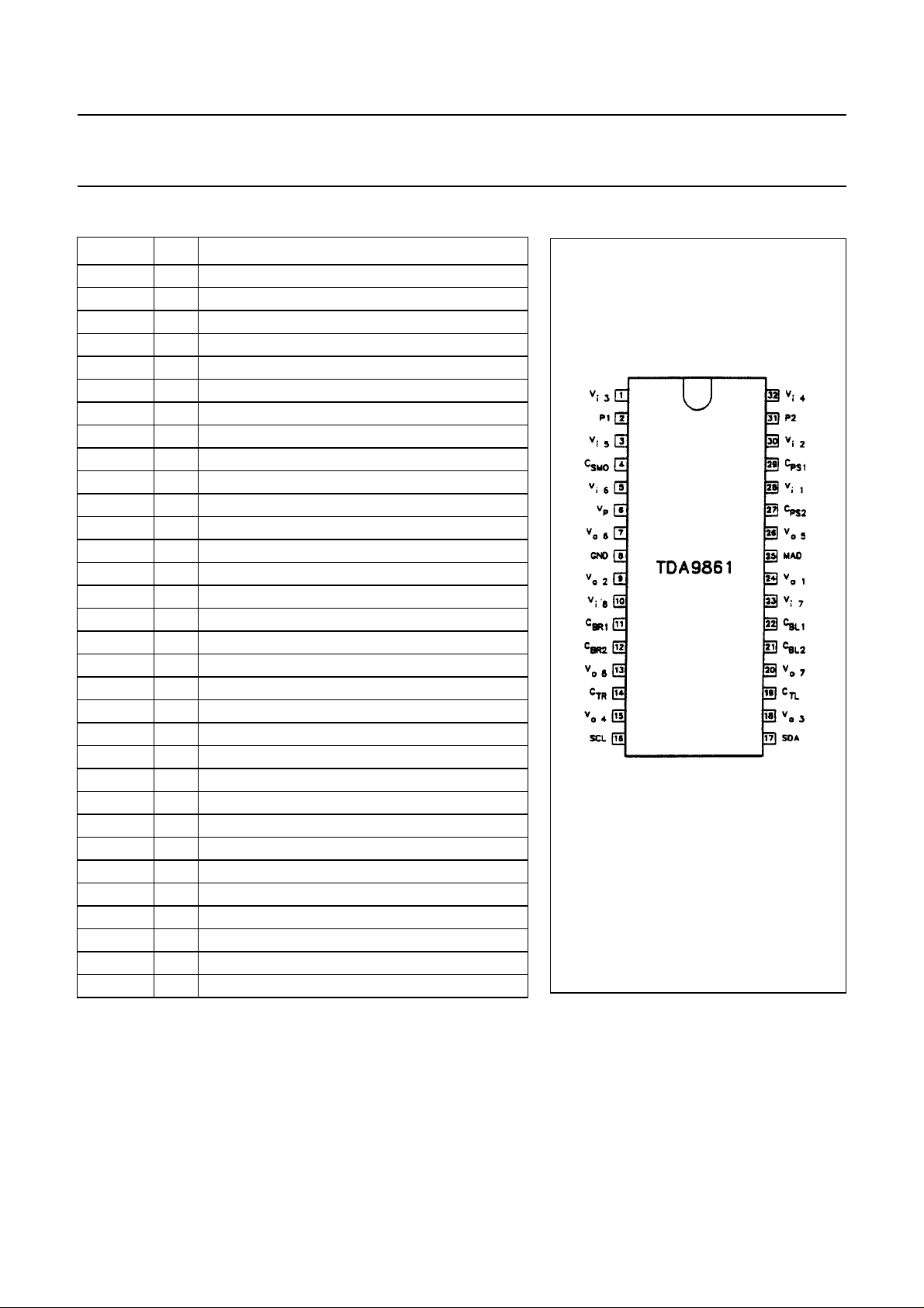
PINNING
SYMBOL PIN DESCRIPTION
V
i 3
P1 2 port 1 output
V
i 5
C
SMO
V
i 6
V
P
V
o 6
GND 8 ground
V
o 2
V
i 8
C
BR1
C
BR2
V
o 8
C
TR
V
o 4
SCL 16 I
SDA 17 I
V
o 3
C
TL
V
o 7
C
BL2
C
BL1
V
i 7
V
o 1
MAD 25 module address select input
V
o 5
C
PS2
V
i 1
C
PS1
V
i 2
P2 31 port 2 output
V
i 4
1 SCART input signal LEFT
3 MAIN input signal LEFT
4 smoothing capacitor of reference voltage
5 MAIN input signal RIGHT
6 positive supply voltage
7 SCART output signal RIGHT
9 MAIN output signal RIGHT
10 input signal RIGHT to loudspeaker channel
11 bass capacitor RIGHT 1
12 bass capacitor RIGHT 2
13 headphone output signal RIGHT
14 treble capacitor RIGHT
15 loudspeaker channel output signal RIGHT
2
C-bus clock line
2
C-bus data line
18 loudspeaker channel output signal LEFT
19 treble capacitor LEFT
20 headphone output signal LEFT
21 bass capacitor LEFT 2
22 bass capacitor LEFT 1
23 input signal LEFT to loudspeaker channel
24 MAIN output signal LEFT
26 SCART output signal LEFT
27 pseudo stereo capacitor 2
28 AUX input signal LEFT
29 pseudo stereo capacitor 1
30 AUX input signal RIGHT
32 SCART input signal RIGHT
Fig.2 Pin configuration.
June 1994 4
Philips Semiconductors Preliminary specification
Universal HiFi audio processor for TV TDA9861
FUNCTIONAL DESCRIPTION
The TDA9861 consists of the following functions:
• source select switching block
• loudspeaker channel with effect controls
• headphone channel
• two port outputs for general purpose
• I2C−bus control
Source select switching block
The TDA9861 selects and switches the input signals from
three stereo or six mono sources as there are MAIN, AUX
and SCART (Fig.1) to one of the outputs SCART,
loudspeaker and headphone (crossbar-switching Table 3).
Due to the fact, that the main channel (LINE outputs) is
looped outside the circuit (from pins 9 and 24 to pins 10
and 23), signals can be used as LINE output or to insert a
‘surround sound decoder’.
Loudspeaker channel
Volume control is divided into the parts volume 1 and
volume 2 / balance. The first part (55 dB) controls left and
right channels simultaneously; the second part (23 dB)
controls volume and balance of left and right channels
independently. Treble control provides a control range
from −12 to +12 dB and bass control from −12 to +15 dB.
Extended bass control can be provided by an external
T-network (Fig.1) from −15 to +19 dB (2 dB steps).
Effect controls
‘Linear stereo’, ‘stereo with spatial effect (30% or 52%
anti-phase crosstalk)’ and ‘forced mono with or without
pseudo-stereo effect’ are controlled by three bits. A muting
of 85 dB is provided.
Headphone channel
The headphone channel is only equipped with volume /
balance control. A muting of 85 dB is provided.
2
I
C-bus control
All settings of control are stored in subaddress registers.
Data transmission is simplified by auto-incrementing the
subaddresses. The on-chip power on reset sets the mute
bit to active, so all 3 stereo outputs are muted.
The muting can be switched off by writing a ‘0’ (non-muted)
into the mute control bits.
LIMITING VALUES
In accordance with the Absolute Maximum Rating System (IEC 134).
SYMBOL PARAMETER MIN. MAX. UNIT
V
P
V
n
I
O
supply voltage (pin 6) 0 10 V
voltage on all pins, ground excluded 0 V
P
output current
at pins 15, 18, 13, 20, 7 and 26 − 2.5 mA
at pins 2 and 31 − 1.5 mA
P
T
T
V
tot
stg
amb
ESD
total power dissipation − 850 mW
storage temperature −25 +150 °C
operating ambient temperature 0 +70 °C
electrostatic handling for all pins (note 1) −±300 V
electrostatic handling for all pins (note 2) −±2000 V
Notes to the Limiting Values
1. Equivalent to discharging a 200 pF capacitor through a 0 Ω series resistor.
2. Equivalent to discharging a 100 pF capacitor through a 1.5 kΩ series resistor.
THERMAL RESISTANCE
SYMBOL PARAMETER THERMAL RESISTANCE
R
th j-a
from junction to ambient in free air 60 K/W
V
June 1994 5
Philips Semiconductors Preliminary specification
Universal HiFi audio processor for TV TDA9861
CHARACTERISTICS
= 8 V; T
V
P
function and forced-mono function in off position and measurements taken in Fig.1 unless otherwise specified.
SYMBOL PARAMETER CONDITIONS MIN. TYP. MAX. UNIT
V
P
I
P
V
ref
V
4
DC voltage on pins
V
i
V
O
V
C
Audio select switch. Line, SCART and headphone outputs (controlled via I
V
i
R
i
f frequency response for all AF outputs −0.5 dB 20 − 20000 Hz
V
o
R
L
G
v
α
cr
LOUDSPEAKER CHANNEL (controlled via I
V olume control 1 (LEFT and RIGHT simultaneously)
V
i
R
i
G
v
∆G
v
= +25 °C; treble and bass in linear positions; balance in mid position; spatial function, pseudo-stereo
amb
supply voltage (pin 6) 7.2 8.0 8.8 V
supply current (pin 6) − 25 − mA
internal reference voltage − VP/2 − V
voltage (pin 4) − VP− 0.1 − V
DC input voltage (pins 1, 3, 5, 10, 23,
− VP/2 − V
28, 30 and 32)
DC output voltage (pins 7, 9, 13, 15, 18,
− VP/2 − V
20, 24 and 26)
DC voltage on capacitors (pins 11, 12,
− VP/2 − V
14, 19, 21, 22, 27 and 29)
2
C-bus, Table 3)
maximum AF input signal on pins 1, 3,
5, 28, 30, 32 (RMS value)
THD ≤ 0.5%
on output pins
2 −−V
input resistance (pins 1, 3, 5, 28, 30, 32) 20 30 40 kΩ
maximum AF output signal on pins 7, 9,
THD ≤ 0.5% 2 −−V
24, 26 (RMS value)
allowed external load resistance
on output (pins 9 and 24) 10 −−kΩ
on output (pins 7 and 26) 5 −−kΩ
gain for all signal arms − 0 − dB
switch crosstalk on outputs between
AF inputs at f = 10 kHz
2
C-bus, Table 3)
unused inputs
connected to ground
− 90 − dB
f = 1 kHz, 55 steps
maximum input signal
(RMS value; pins 10 and 23)
Gv= 0; THD ≤ 0.5% on
output pins 15 and 18
2 −−V
input resistance (pins 10 and 23) 7.5 10 − kΩ
nominal volume control −40 − +15 dB
minimum volume control −38 − +14 dB
step width Gv= −32 to +15 dB 0.5 1.0 1.5 dB
= −40 to −33 dB 0.25 1.0 1.75 dB
G
v
gain set error G
= −32 to +15 dB −− 1dB
v
G
=−40 to −33 dB −− 2dB
v
June 1994 6
 Loading...