

Philips TDA9859 Technical data
INTEGRATED CIRCUITS
DATA SH EET
TDA9859
Universal hi-fi audio processor for
TV
Product specification
Supersedes data of 2001 Jul 02
File under Integrated Circuits, IC02
2001 Jul 11
Philips Semiconductors Product specification
Universal hi-fi audio processor for TV TDA9859
FEATURES
• Multi-source selector switches six AF inputs
(three stereo sources or six mono sources)
• Each ofthe input signals can be switched to each of the
outputs (crossbar switch)
• Outputs for loudspeaker channel and peri-TV connector
(SCART)
• Switchable spatial stereo and pseudo stereo effects
• Audio surround decoder can be added externally
• Two general purpose logic output ports
• I2C-bus control of all functions.
QUICK REFERENCE DATA
SYMBOL PARAMETER MIN. TYP. MAX. UNIT
V
P
I
P
V
i(rms)
V
o(rms)
G
v
positive supply voltage (pin VP) 7.2 8.0 8.8 V
supply current − 25 − mA
input signal levels for 0 dB gain (RMS value) 2 −−V
output signal levels for 0 dB gain (RMS value) 2 −−V
voltage gain in main channel
volume control (in 1 dB steps, balance included) −63 − +15 dB
mute −80 −−dB
bass control (in 1.5 dB steps) −12 − +15 dB
treble control (in 3 dB steps) −12 − +12 dB
THD total harmonic distortion − 0.1 − %
S/N signal-to-noise ratio − 85 − dB
T
amb
ambient temperature 0 − 70 °C
GENERAL DESCRIPTION
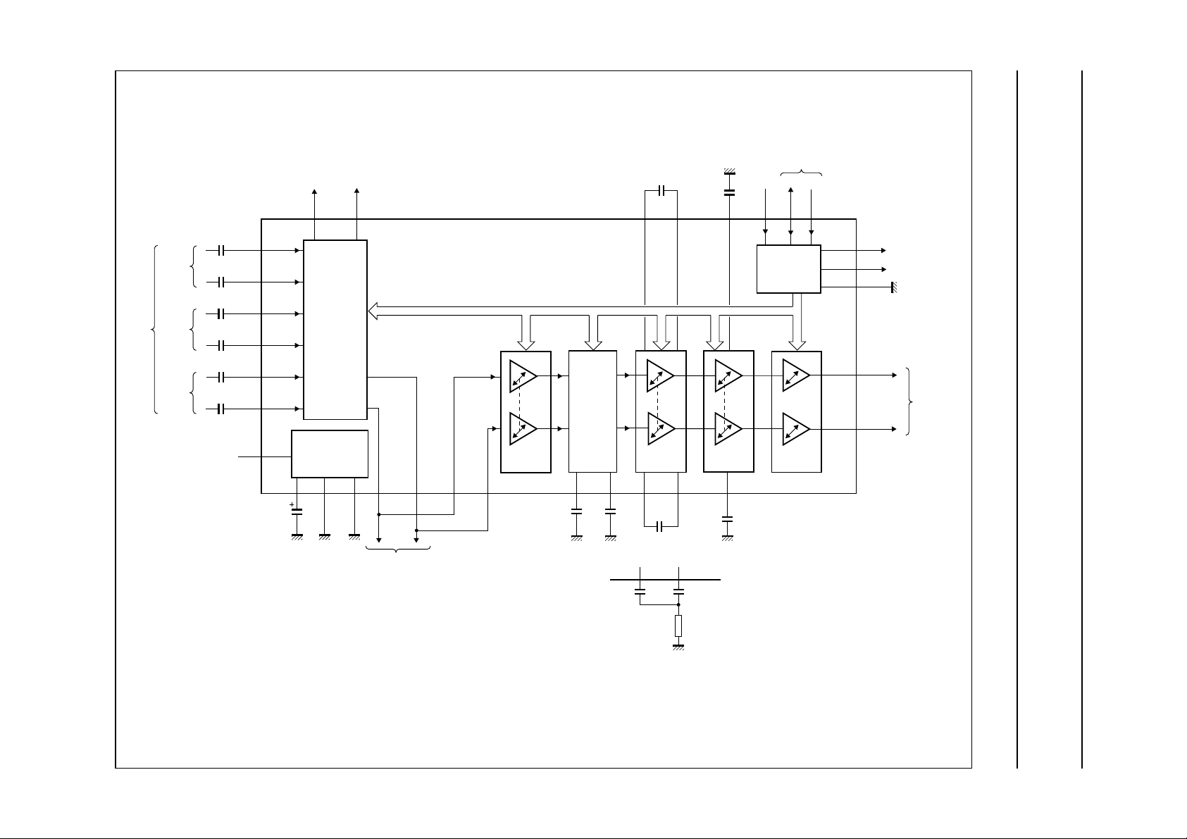
The TDA9859 provides control facilities for the main and
the SCART channel of a TV set. Due to extended
switching possibilities, signals from three stereo sources
can be handled.
ORDERING INFORMATION
TYPE
NUMBER
NAME DESCRIPTION VERSION
PACKAGE
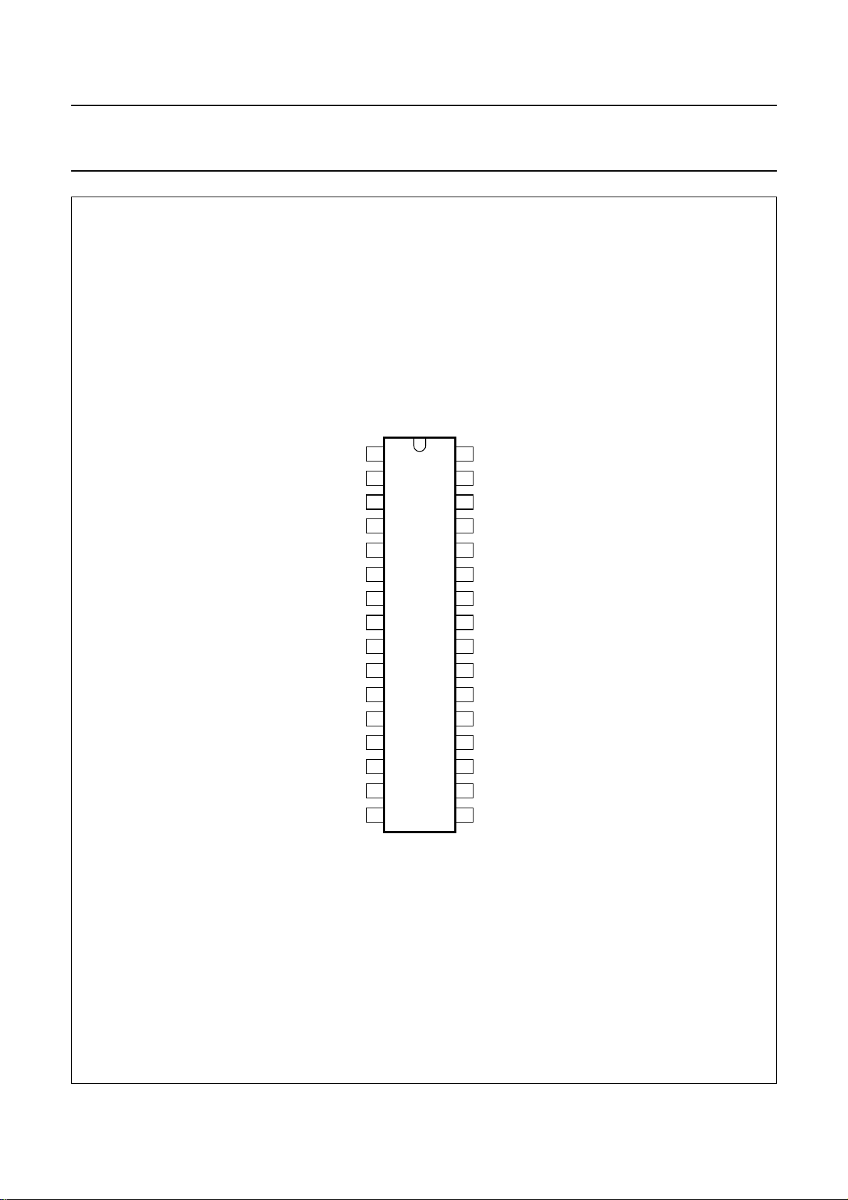
TDA9859 SDIP32 plastic shrink dual in-line package; 32 leads (400 mil) SOT232-1
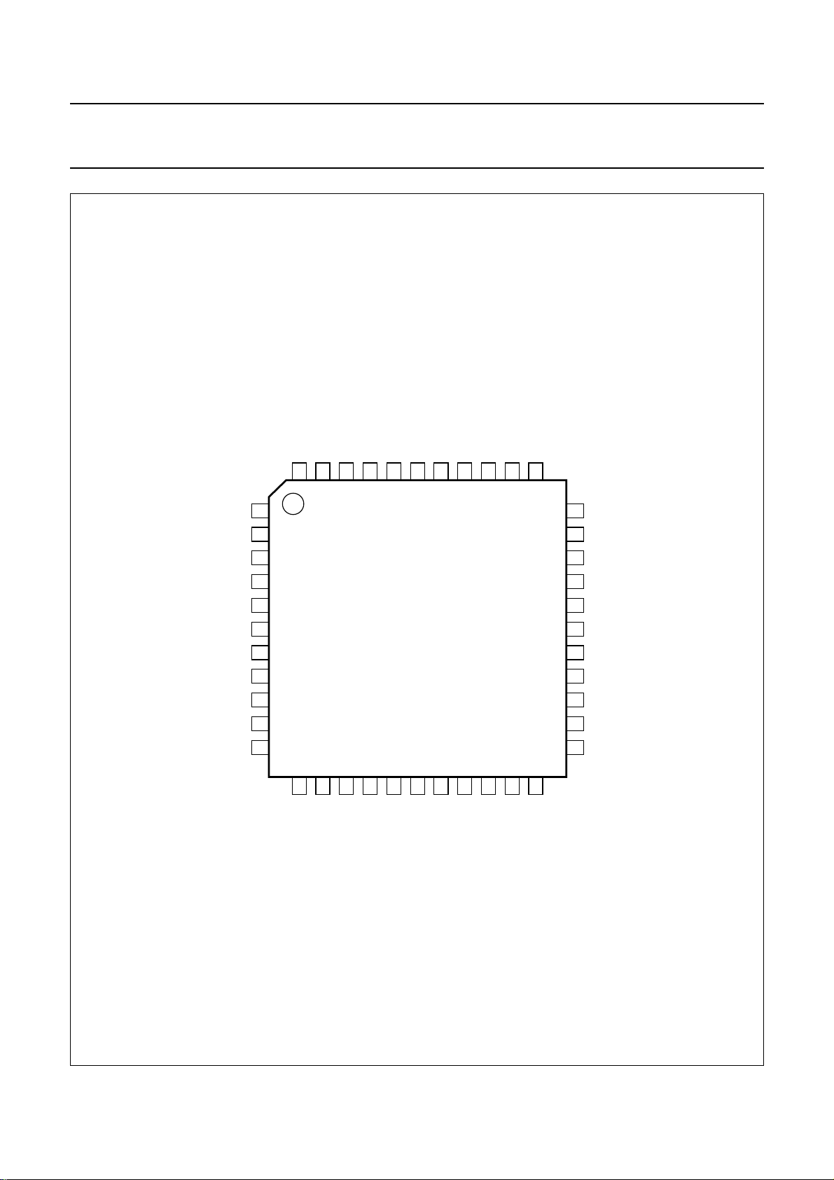
TDA9859H QFP44 plastic quad flat package; 44 leads (lead length 1.3 mm);
SOT307-2
body 10 × 10 × 1.75 mm
2001 Jul 11 2
This text is here in white to force landscape pages to be rotated correctly when browsing through the pdf in the Acrobat reader.This text is here in
f
_white to force landscape pages to be rotated correctly when browsing through the pdf in the Acrobat reader.This text is here inThis text is here in
white to force landscape pages to be rotated correctly when browsing through the pdf in the Acrobat reader. white to force landscape pages to be ...
2001 Jul 11 3
SCART
output
LR
audio
inputs
AUX
SCART
MAIN
L
R
L
R
L
R
470 nF
470 nF
470 nF
470 nF
470 nF
470 nF
+8 V
AIN
L
AIN
R
SCIN
L
SCIN
R
MIN
L
MIN
R
V
P
28 (43)
30 (3)
1 (7)
32 (5)
3 (9)
5 (13)
6 (14)
C
SMO
SCOUTLSCOUT
26 (41) 7 (15)
MULTIPLE
SOURCE
AND MODE
SELECTOR
(CROSSBAR
SWITCH)
REFERENCE
VOLTAGE
(16)
4 (10)
AGND
100
µF
LINE output or optional
surround sound decoder
R
8
24 (38) 9 (18)
MOUT
GND
LR
connection
L
MOUT
TDA9859
(TDA9859H)
23 (37) 10 (19)
LINLLIN
R
ull pagewidth
VOLUME
CONTROL
R
STEREO
SPATIAL
STEREO
PSEUDO
STEREO
FORCED
MONO
29 (2) 27 (42)
C
PS1CPS2
extended bass control
68 nF
33 nF
C
BL1
22 (36) 21 (35)
BASS
CONTROL
11 (20) 12 (21)
C
33 nF
11 (22) 12 (21)
(1)
C
BL2
BR1CBR2
(1)
0.15 µF
5.6 nF
TREBLE
CONTROL
C
TR
(1)
MAD SDA SCL
C
TL
19 (31) 25
INTERFACE
14 (25)
5.6 nF
2
C-bus
I
(40)17(29)
2
I
C-BUS
MUTE
VOLUME
BALANCE
16 (27)
(4) 31
(30) 18
(26) 15
(8) 2
(17)
DGND
LOUT
LOUT
MHB917
P2
P1
L
L
R
R
loudspeaker
channel
outputs
BLOCK DIAGRAM
Philips Semiconductors Product specification
Universal hi-fi audio processor for TV TDA9859
The pin numbers given in parenthesis refer to the TDA9859H version.
(1) For extended bass control, the capacitor between C
BR/L1
and C
Fig.1 Block diagram and application circuit.
13 kΩ
should be replaced by the extended bass control network.
BR/L2
Philips Semiconductors Product specification
Universal hi-fi audio processor for TV TDA9859
PINNING
PIN
SYMBOL
DESCRIPTION
TDA9859 TDA9859H
SCIN
L
1 7 SCART input;
left channel
P1 2 8 port 1 output
MIN
L
3 9 MAIN input;
left channel
C
SMO
4 10 smoothing
capacitor of
reference voltage
n.c. − 11 not connected
n.c. − 12 not connected
MIN
R
5 13 MAIN input;
right channel
V
P
SCOUT
R
6 14 supply voltage
7 15 SCART output;
right channel
GND 8 − ground
AGND − 16 analog ground
DGND − 17 digital ground
MOUT
R
9 18 MAIN output;
right channel
LIN
R
10 19 input to right
loudspeaker
channel
C
BR1
11 20 bass capacitor
connection 1;
right channel
C
BR2
12 21 bass capacitor
connection 2;
right channel
n.c. − 22 not connected
n.c. − 23 not connected
n.c. 13 24 not connected
C
TR
14 25 treble capacitor
connection;
right channel
LOUT
R
15 26 loudspeaker output;
right channel
SCL 16 27 serial clock input;
2
I
C-bus
n.c. − 28 not connected
SYMBOL
DESCRIPTION
TDA9859 TDA9859H
SDA 17 29 serial data
input/output;
I2C-bus
PIN
LOUT
L
18 30 loudspeaker output;
left channel
C
TL
19 31 treble capacitor
connection;
left channel
n.c. 20 32 not connected
n.c. − 33 not connected
n.c. − 34 not connected
C
BL2
21 35 bass capacitor
connection 2;
left channel
C
BL1
22 36 bass capacitor
connection 1;
left channel
LIN
L
23 37 input to left
loudspeaker
channel
MOUT
L
24 38 MAIN output;
left channel
n.c. − 39 not connected
MAD 25 40 module address
select input
SCOUT
L
26 41 SCART output;
left channel
C
PS2
27 42 pseudo stereo
capacitor 2
AIN
L
28 43 AUX input;
left channel
n.c. − 44 not connected
n.c. − 1 not connected
C
PS1
29 2 pseudo stereo
capacitor 1
AIN
R
30 3 AUX input;
right channel
P2 31 4 port 2 output
SCIN
R
32 5 SCARTinput signal
RIGHT
n.c. − 6 not connected
2001 Jul 11 4
Philips Semiconductors Product specification
Universal hi-fi audio processor for TV TDA9859
handbook, halfpage
SCOUT
SCIN
MIN
C
SMO
MIN
GND
MOUT
LIN
C
BR1
C
BR2
C
LOUT
SCL
P1
V
n.c.
TR
1
L
2
3
L
4
5
R
6
P
7
R
8
TDA9859
9
R
10
R
11
12
13
14
15
R
16
MHA779
32
31
30
29
28
27
26
25
24
23
22
21
20
19
18
17
SCIN
P2
AIN
R
C
PS1
AIN
L
C
PS2
SCOUT
MAD
MOUT
LIN
L
C
BL1
C
BL2
n.c.
C
TL
LOUT
SDA
R
L
L
L
Fig.2 Pin configuration TDA9859 SDIP32 version.
2001 Jul 11 5
Philips Semiconductors Product specification
Universal hi-fi audio processor for TV TDA9859
handbook, full pagewidth
C
PS1
AIN
SCIN
SCIN
MIN
C
SMO
n.c.
P2
n.c.
P1
n.c.
AINLC
43
13
R
MIN
42
14
V
PS2
P
SCOUTLMAD
41
40
TDA9859H
15
16
R
AGND
SCOUT
n.c.
39
17
DGND
MOUTLLINLC
38
18
R
MOUT
n.c.
44
1
2
3
R
4
5
R
6
7
L
8
9
L
10
11
12
n.c.
37
19
R
LIN
BL1CBL2
36
35
20
21
BR1CBR2
C
n.c.
34
22
n.c.
33
n.c.
32
n.c.
31
C
30
LOUT
29
SDA
28
n.c.
27
SCL
26
LOUT
25
C
24
n.c.
23
n.c.
MHB918
TL
L
R
TR
Fig.3 Pin configuration TDA9859H QFP44 version.
2001 Jul 11 6
Philips Semiconductors Product specification
Universal hi-fi audio processor for TV TDA9859
FUNCTIONAL DESCRIPTION
The TDA9859 consists of the following functions:
• Source select switching block
• Loudspeaker channel with effect controls
• Two port outputs for general purpose
• I2C-bus control.
Source select switching block
The TDA9859 selects and switches the input signals from
three stereo or six mono sources MAIN, AUX and SCART
(see Fig.1) to the outputs SCART and loudspeaker
(crossbar-switching; Table 4). The main channel (LINE
outputs) is looped outside the circuit (from pins MOUT
R
and MOUTL to pins LINR and LINL), so signals can be
used as LINE output or a surround sound decoder can be
inserted.
Effect controls
‘Linear stereo’, ‘stereo with spatial effect (30% or 52%
anti-phase crosstalk)’ and ‘forced mono with or without
pseudo-stereoeffect’arecontrolledbythreebits.Amuting
of 85 dB is provided.
Loudspeaker channel
Volumecontrol is divided into volume control common and
volume control left/right. The common part
(−40 to +15 dB) controls the left and right channels
simultaneously;theleft/rightpart (−23 to 0 dB) controlsthe
volume of left and right channels independently. Treble
control provides a control range from −12 to +12 dB and
bass control from −12 to +15 dB. Extended bass control
can be provided by an external T-network (see Fig.1) from
−15 to +19 dB (in 2 dB steps).
2
C-bus control
I
All control settings are stored in subaddress registers.
Data transmission is simplified by auto-incrementing the
subaddresses. The on-chip Power-on reset sets the mute
bit to active, so both the SCART and the loudspeaker
outputs are muted.
Themutingcanbeswitchedoff by writing a ‘0’(non-muted)
into the mute control bits.
LIMITING VALUES
In accordance with the Absolute Maximum Rating System (IEC 60134).
SYMBOL PARAMETER CONDITIONS MIN. MAX. UNIT
V
P
V
n
I
O
supply voltage (pin VP) − 010V
voltage on all pins, ground excluded − 0V
P
V
output current
at LOUT and SCOUT pins −−2.5 mA
at port output pins −−1.5 mA
P
tot
T
amb
T
stg
V
es
total power dissipation −−850 mW
ambient temperature − 070°C
storage temperature −−25 +150 °C
electrostatic handling voltage all pins; note 1 −±300 V
all pins; note 2 −±2000 V
Notes
1. Equivalent to discharging a 200 pF capacitor through a 0 Ω series resistor (machine model).
2. Equivalent to discharging a 100 pF capacitor through a 1.5 kΩ series resistor (human body model).
2001 Jul 11 7
Philips Semiconductors Product specification
Universal hi-fi audio processor for TV TDA9859
THERMAL CHARACTERISTICS
SYMBOL PARAMETER CONDITIONS VALUE UNIT
R
th(j-a)
CHARACTERISTICS
V
=8V; T
P
pseudo-stereo function and forced-mono function in off position and measurements taken in Fig.1; unless otherwise
specified.
SYMBOL PARAMETER CONDITIONS MIN. TYP. MAX. UNIT
V
P
I
P
V
ref
V
SMO
DC voltage on pins
V
I
V
O
V
C
Audio select switch; line and SCART outputs (controlled via I
V
i(rms)
R
i
B
−0.5 dB
V
o(rms)
R
L
G
v
α
cr
thermal resistance from junction to ambient in free air
TDA9859 (SDIP32) 60 K/W
TDA9859H (QFP44) 65 K/W
=25°C; treble and bass in linear positions (0 dB); volume control left/right 0 dB; spatial function,
amb
supply voltage (pin VP) 7.2 8.0 8.8 V
supply current (pin VP) − 25 − mA
internal reference voltage − 0.5V
voltage at pin C
SMO
DC input voltage at pins SCIN, MIN,
− VP− 0.1 − V
− 0.5V
P
P
− V
− V
LIN and AIN
DC output voltage at pins SCOUT,
− 0.5V
P
− V
MOUT and LOUT
DC voltage on capacitors (pins C
C
, CTR, CTL, C
BR2
and C
PS1
)
BL2
, C
BL1
, C
maximum AF input signal on
pins SCIN, MIN and AIN (RMS value)
input resistance at pins SCIN, MIN and
PS2
BR1
,
2
THD ≤ 0.5% on output
pins
− 0.5V
C-bus); see Table 4
2 −−V
20 30 40 kΩ
P
− V
AIN
−0.5 dB bandwidth for pins SCOUT,
20 − 20000 Hz
MOUT and LOUT
maximum AF output signal on
THD ≤ 0.5% 2 −−V
pins SCOUT and MOUT (RMS value)
allowed external load resistance
on output pins MOUT 10 −−kΩ
on output pins SCOUT 5 −−kΩ
voltage gain from any input to SCART
− 0 − dB
and MAIN outputs
switch crosstalk on outputs between
AF inputs
f = 10 kHz; unused inputs
connected to ground
− 90 − dB
2001 Jul 11 8
 Loading...