Philips TDA9859 Datasheet

INTEGRATED CIRCUITS
DATA SH EET
TDA9859
Universal hi-fi audio processor for
TV
Preliminary specification
File under Integrated Circuits, IC02
1997 Sep 01

Philips Semiconductors Preliminary specification
Universal hi-fi audio processor for TV TDA9859
FEATURES
• Multi-source selector switches six AF inputs
(three stereo sources or six mono sources)
• Each of the input signals can be switched to each of the
outputs (crossbar switch)
• Outputs for loudspeaker channel and peri-TV connector
(SCART)
• Switchable spatial stereo and pseudo stereo effects
• Audio surround decoder can be added externally
• Two general purpose logic output ports
2
C-bus control of all functions.
• I
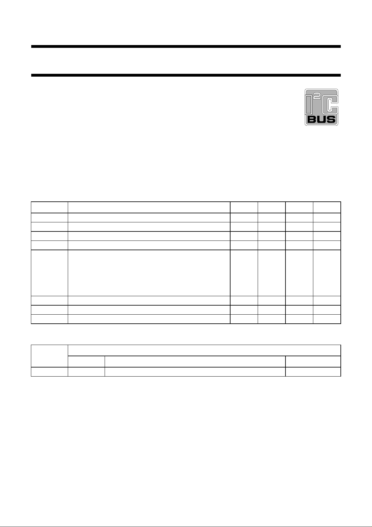
QUICK REFERENCE DATA
SYMBOL PARAMETER MIN. TYP. MAX. UNIT
V
P
I
P
V
i(rms)
V
o(rms)
G
v
positive supply voltage (pin 6) 7.2 8.0 8.8 V
supply current − 25 − mA
input signal levels for 0 dB gain (RMS value) 2 −−V
output signal levels for 0 dB gain (RMS value) 2 −−V
voltage gain in main channel
volume control (1 dB steps, balance included) −63 − +15 dB
mute −80 −−dB
bass control (1.5 dB steps) −12 − +15 dB
treble control (3 dB steps) −12 − +12 dB
THD total harmonic distortion − 0.1 − %
S/N signal-to-noise ratio − 85 − dB
T
amb
operating ambient temperature 0 − 70 °C
GENERAL DESCRIPTION
The TDA9859 provides control facilities for the main and
the SCART channel of a TV set. Due to extended
switching possibilities, signals from three stereo sources
can be handled.
ORDERING INFORMATION
TYPE
NUMBER
NAME DESCRIPTION VERSION
PACKAGE
TDA9859 SDIP32 plastic shrink dual in-line package; 32 leads (400 mil) SOT232-1
1997 Sep 01 2

Philips Semiconductors Preliminary specification
Universal hi-fi audio processor for TV TDA9859
BLOCK DIAGRAM
outputs
channel
loudspeaker
C-bus
2
I
MAD SDA SCL
33 nF
5.6 nF
(1)
C
C
C
TL
BL2
BL1
P1
P2
2
31
C-BUS
2
I
INTERFACE
19 25 17 16
22 21
L
L
LOUT
18
STEREO
SPATIAL
MUTE
PSEUDO
STEREO
R
R
LOUT
15
STEREO
VOLUME
BALANCE
TREBLE
CONTROL
BASS
CONTROL
MONO
FORCED
14
11 12
29 27
MHA778
BR2
C
(1)
BR1
C
5.6 nF
TR
(1)
C
33 nF
PS2
extended bass control
C
PS1
C
11 (22) 12 (21)
0.15 µF
13 kΩ
68 nF
width
R
SCOUT
L
output
SCART
LR
SCOUT
VOLUME
CONTROL
R
23 10
24 9
48
VOLTAGE
LIN
L
LIN
R
MOUT
L
MOUT
LR
GND
100
C
SMO
LINE output or optional
µF
connection
surround sound decoder
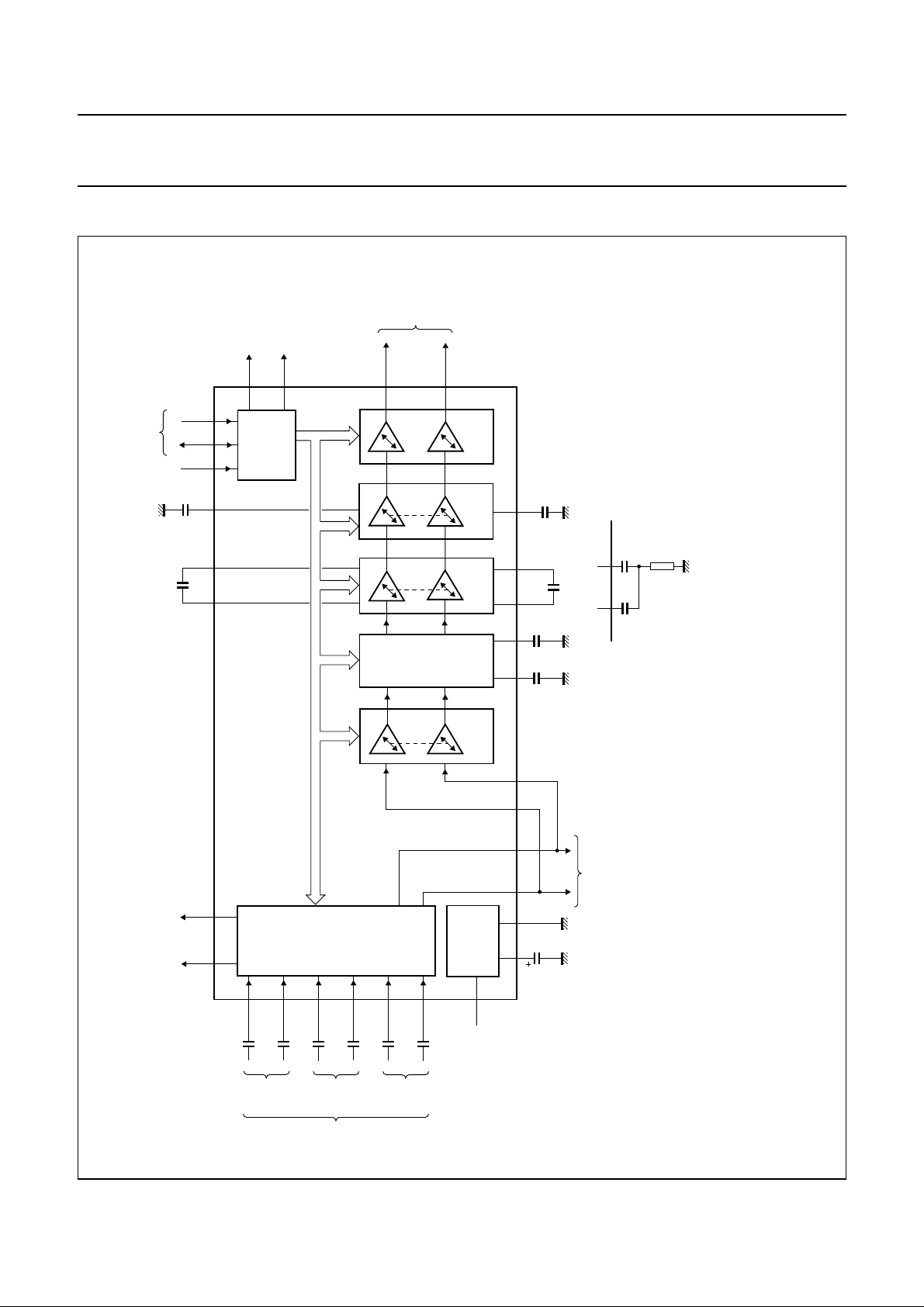
should be replaced by the extended bass control network.
BR/L2
Fig.1 Block diagram and application circuit.
and C
BR/L1
(1) For extended bass control, the capacitor between C
TDA9859
26 7
28
L
AIN
L
30
R
AIN
470 nF
AUX
SOURCE
MULTIPLE
AND MODE
1
L
SCIN
470 nF
L
R
SELECTOR
470 nF
SCART
audio
32
R
SCIN
R
inputs
SWITCH)
(CROSSBAR
3
L
MIN
470 nF
470 nF
L
5
R
MIN
MAIN
R
470 nF
REFERENCE
6
P
V
+8 V
1997 Sep 01 3

Philips Semiconductors Preliminary specification
Universal hi-fi audio processor for TV TDA9859
PINNING
SYMBOL PIN DESCRIPTION
SCIN
L
P1 2 port 1 output
MIN
L
C
SMO
MIN
R
V
P
SCOUT
GND 8 ground
MOUT
LIN
R
C
BR1
C
BR2
n.c. 13 not connected
C
TR
LOUT
R
SCL 16 serial clock input; I
SDA 17 serial data input/output; I
LOUT
L
C
TL
n.c. 20 not connected
C
BL2
C
BL1
LIN
L
MOUT
MAD 25 module address select input
SCOUT
C
PS2
AIN
L
C
PS1
AIN
R
P2 31 port 2 output
SCIN
R
1 SCART input; left channel
3 MAIN input; left channel
smoothing capacitor of reference
4
voltage
5 MAIN input; right channel
6 supply voltage
7 SCART output; right channel
R
9 MAIN output; right channel
R
10 input to right loudspeaker channel
bass capacitor connection 1;
11
right channel
bass capacitor connection 2;
12
right channel
treble capacitor connection;
14
right channel
15 loudspeaker output; right channel
2
18 loudspeaker output; left channel
treble capacitor connection;
19
left channel
bass capacitor connection 2;
21
left channel
bass capacitor connection 1;
22
left channel
23 input to left loudspeaker channel
24 MAIN output; left channel
L
26 SCART output; left channel
L
27 pseudo stereo capacitor 2
28 AUX input; left channel
29 pseudo stereo capacitor 1
30 AUX input; right channel
32 SCART input signal RIGHT
C-bus
2
C-bus
handbook, halfpage
SCOUT
SCIN
1
L
P1
2
MIN
3
L
C
4
SMO
MIN
5
R
V
6
P
7
R
GND
8
MOUT
LIN
C
C
C
LOUT
BR1
BR2
n.c.
TR
SCL
TDA9859
9
R
10
R
11
12
13
14
15
R
16
MHA779
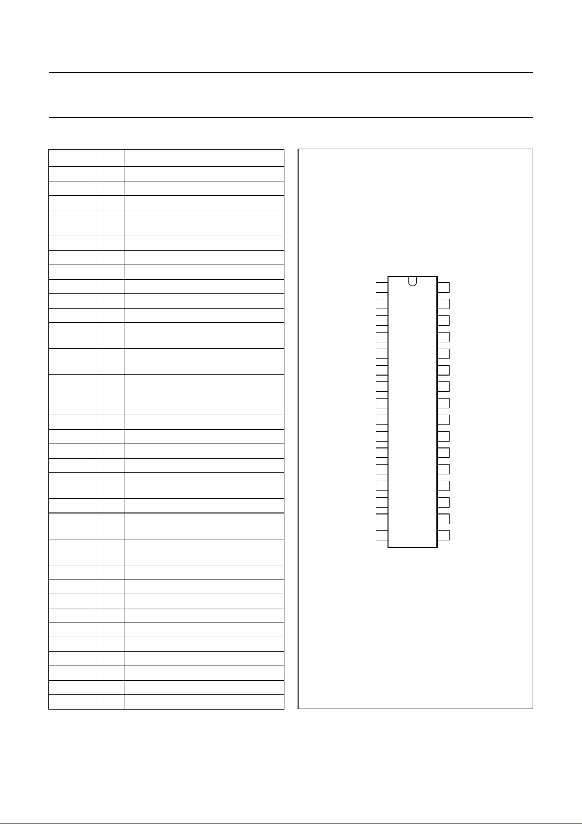
Fig.2 Pin configuration.
32
31
30
29
28
27
26
25
24
23
22
21
20
19
18
17
SCIN
P2
AIN
R
C
PS1
AIN
L
C
PS2
SCOUT
MAD
MOUT
LIN
L
C
BL1
C
BL2
n.c.
C
TL
LOUT
SDA
R
L
L
L
1997 Sep 01 4

Philips Semiconductors Preliminary specification
Universal hi-fi audio processor for TV TDA9859
FUNCTIONAL DESCRIPTION
The TDA9859 consists of the following functions:
• Source select switching block
• Loudspeaker channel with effect controls
• Two port outputs for general purpose
• I2C-bus control.
Source select switching block
simultaneously; the left/right part (−23 to 0 dB) controls the
volume of left and right channels independently. Treble
control provides a control range from −12 to +12 dB and
bass control from −12 to +15 dB. Extended bass control
can be provided by an external T-network (see Fig.1) from
−15 to +19 dB (2 dB steps).
Effect controls
‘Linear stereo’, ‘stereo with spatial effect (30% or 52%
anti-phase crosstalk)’ and ‘forced mono with or without
The TDA9859 selects and switches the input signals from
three stereo or six mono sources MAIN, AUX and SCART
pseudo-stereo effect’ are controlled by three bits. A muting
of 85 dB is provided.
(see Fig.1) to the outputs SCART and loudspeaker
(crossbar-switching; Table 4). The main channel (LINE
outputs) is looped outside the circuit (from pins 9 and 24 to
pins 10 and 23), so signals can be used as LINE output or
a surround sound decoder can be inserted.
2
I
C-bus control
All settings of control are stored in subaddress registers.
Data transmission is simplified by auto-incrementing the
subaddresses. The on-chip Power-on reset sets the mute
Loudspeaker channel
Volume control is divided into volume control common and
volume control left/right. The common part
(−40 to +15 dB) controls the left and right channels
bit to active, so both the SCART and the loudspeaker
outputs are muted.
The muting can be switched off by writing a ‘0’ (non-muted)
into the mute control bits.
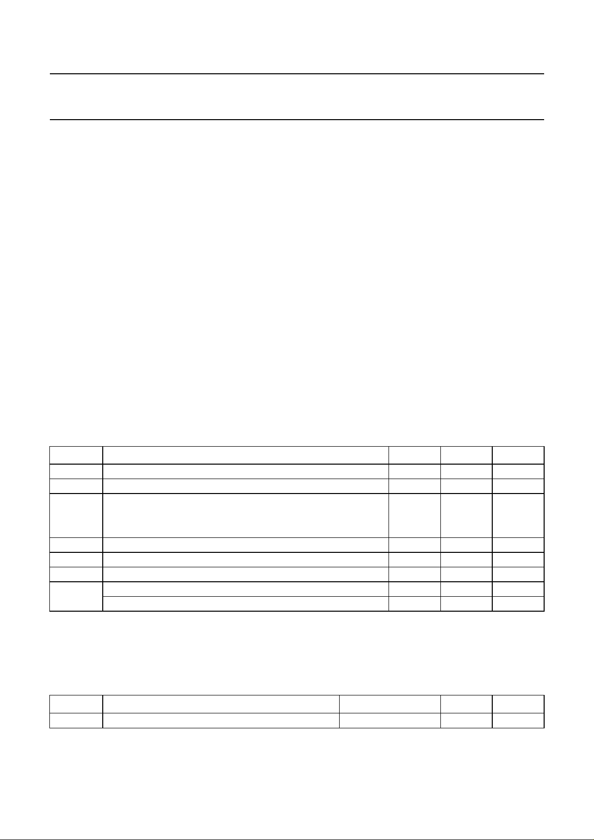
LIMITING VALUES
In accordance with the Absolute Maximum Rating System (IEC 134).
SYMBOL PARAMETER MIN. MAX. UNIT
V
P
V
n
I
O
supply voltage (pin 6) 0 10 V
voltage on all pins, ground excluded 0 V
P
output current
V
at LOUT and SCOUT pins − 2.5 mA
at port output pins − 1.5 mA
P
tot
T
amb
T
stg
V
es
total power dissipation − 850 mW
operating ambient temperature 0 70 °C
storage temperature −25 +150 °C
electrostatic handling for all pins; note 1 −±300 V
electrostatic handling for all pins; note 2 −±2000 V
Notes
1. Equivalent to discharging a 200 pF capacitor through a 0 Ω series resistor (Machine Model).
2. Equivalent to discharging a 100 pF capacitor through a 1.5 kΩ series resistor (Human Body Model).
THERMAL CHARACTERISTICS
SYMBOL PARAMETER CONDITIONS VALUE UNIT
R
th(j-a)
thermal resistance from junction to ambient in free air 60 K/W
1997 Sep 01 5

Philips Semiconductors Preliminary specification
Universal hi-fi audio processor for TV TDA9859
CHARACTERISTICS
VP=8V; T
pseudo-stereo function and forced-mono function in off position and measurements taken in Fig.1; unless otherwise
specified.
SYMBOL PARAMETER CONDITIONS MIN. TYP. MAX. UNIT
V
P
I
P
V
ref
V
4
DC voltage on pins
V
I
V
O
V
C
Audio select switch; line and SCART outputs (controlled via I
V
i(rms)
R
i
B
−0.5 dB
V
o(rms)
R
L
G
v
α
cr
=25°C; treble and bass in linear positions (0 dB); volume control left/right 0 dB; spatial function,
amb
supply voltage (pin 6) 7.2 8.0 8.8 V
supply current (pin 6) − 25 − mA
internal reference voltage − 0.5V
P
− V
voltage at pin 4 − VP− 0.1 − V
DC input voltage at pins 1, 3, 5, 10, 23,
− 0.5V
P
− V
28, 30 and 32 (inputs SCIN, MIN, LIN
and AIN)
DC output voltage at pins 7, 9, 15, 18,
− 0.5V
P
− V
24, 26 (outputs SCOUT, MOUT
and LOUT)
DC voltage on capacitors (pins 11, 12,
− 0.5V
P
− V
14, 19, 21, 22, 27 and 29)
2
C-bus); see Table 4
maximum AF input signal on
pins SCIN, MIN and AIN (RMS value)
input resistance (pins SCIN, MIN and
THD ≤ 0.5% on output
pins
2 −−V
20 30 40 kΩ
AIN)
−0.5 dB bandwidth for pins SCOUT,
20 − 20 000 Hz
MOUT and LOUT.
maximum AF output signal on
THD ≤ 0.5% 2 −−V
pins SCOUT and MOUT (RMS value)
allowed external load resistance
on output (pins MOUT) 10 −−kΩ
on output (pins SCOUT) 5 −−kΩ
voltage gain from any input to SCART
− 0 − dB
and MAIN outputs
switch crosstalk on outputs between
AF inputs at f = 10 kHz
unused inputs connected
to ground
− 90 − dB
Volume control common (f = 1 kHz, 55 steps)
V
i(rms)
R
i
G
v
maximum input signal (RMS value;
pins LIN)
Gv= 0; THD ≤ 0.5% on
output pins 15 and 18
input resistance (pins LIN) 7.5 10 − kΩ
volume control common voltage gain
nominal −40 − +15 dB
minimum −38 − +14 dB
1997 Sep 01 6
2 −−V
 Loading...