

Philips TDA8793HL-C1 Datasheet

DATA SH EET
Preliminary specification
Supersedes data of 1998 May 14
File under Integrated Circuits, IC02
1999 Oct 06
INTEGRATED CIRCUITS
TDA8793
8-bit, low-power, 3 V, 100 Msps
Analog-to-Digital Converter (ADC)
1999 Oct 06 2
Philips Semiconductors Preliminary specification
8-bit, low-power, 3 V, 100 Msps
Analog-to-Digital Converter (ADC)
TDA8793
FEATURES
• 8-bit low-power ADC (170 mW typical)
• 2.7 to 3.6 V operation
• Sampling rate up to 100 Msps
• Track-and-hold circuit
• CMOS/TTL compatible digital inputs and outputs
• Internal references
• Adjustable full scale range possibility with external
reference
• Power-down mode; 5 mW.
APPLICATIONS
• Radio communications
• Digital data storage read channels
• Medical imaging
• Digital instrumentation.
GENERAL DESCRIPTION
The TDA8793 is an 8-bit low-power Analog-to-Digital
Converter (ADC) which includes a track-and-hold circuit
and internal references. The device converts an analog
input signal, up to 100 MHz, into 8-bit binary codes at a
maximum sample rate of 100 Msps. All digital inputs and
outputareTTL/CMOScompatible.Asinewaveclockinput
signal can also by used.
The Power-down mode enables the device power
consumption to be reduced to 5 mW.
QUICK REFERENCE DATA
ORDERING INFORMATION
SYMBOL PARAMETER CONDITIONS MIN. TYP. MAX. UNIT
V
CCA
analog supply voltage 2.7 3.0 3.6 V
V
CCD
digital supply voltage 2.7 3.0 3.6 V
V
CCO
output stages supply voltage 2.7 3.0 3.6 V
I
CCA
analog supply current operating 32 40 48 mA
standby 0 5 100 µA
I
CCD
digital supply current operating 13 16 22 mA
standby 0 0.65 1.1 mA
I
CCO
output stages supply current − 0.1 − mA
INL integral non-linearity ramp input; f
CLK
= 2 MHz;
V
CCA=VCCD
=3V
−±0.8 tbf LSB
DNL differential non-linearity ramp input; f
CLK
= 2 MHz;
V
CCA=VCCD
=3V
−±0.25 tbf LSB
f
CLK(max)
maximum clock input frequency 100 −−MHz
P
tot
total power dissipation VCC=3V − 170 − mW
TYPE
NUMBER
PACKAGE
NAME DESCRIPTION VERSION
TDA8793HL LQFP32 plastic low profile quad flat package; 32 leads; body 5 × 5 × 1.4 mm SOT401-1
1999 Oct 06 3
Philips Semiconductors Preliminary specification
8-bit, low-power, 3 V, 100 Msps
Analog-to-Digital Converter (ADC)
TDA8793
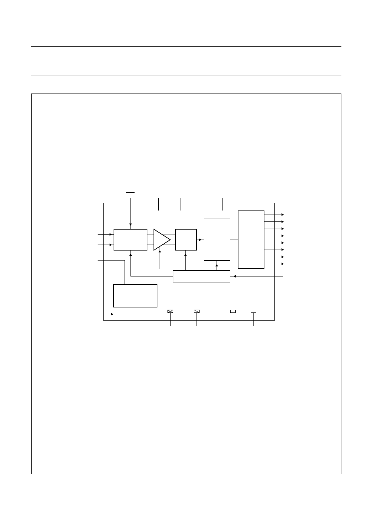
BLOCK DIAGRAM
handbook, full pagewidth
MGR016
TRACK-AND-
HOLD
ADC
LATCHES
CMOS
OUTPUTS
V
REFOUT
= 1.85 V
V
SDN
= 1.25 V
REFERENCE
3
4
INN
5
REFOUT
2
REFIN
32
SDN
8
STDBY
INP
D7
26
D6
25
D5
24
D4
23
D3
18
D2
17
D1
16
D0
15
CLK
11
12
TEN
DEC
31
AGND
6
7
V
CCA
10
V
CCD
22
V
CCO2
20
V
CCO1
CLOCK DRIVER
DGND
9
OGND119ODGND2
21
TDA8793
Fig.1 Block diagram.
1999 Oct 06 4
Philips Semiconductors Preliminary specification
8-bit, low-power, 3 V, 100 Msps
Analog-to-Digital Converter (ADC)
TDA8793
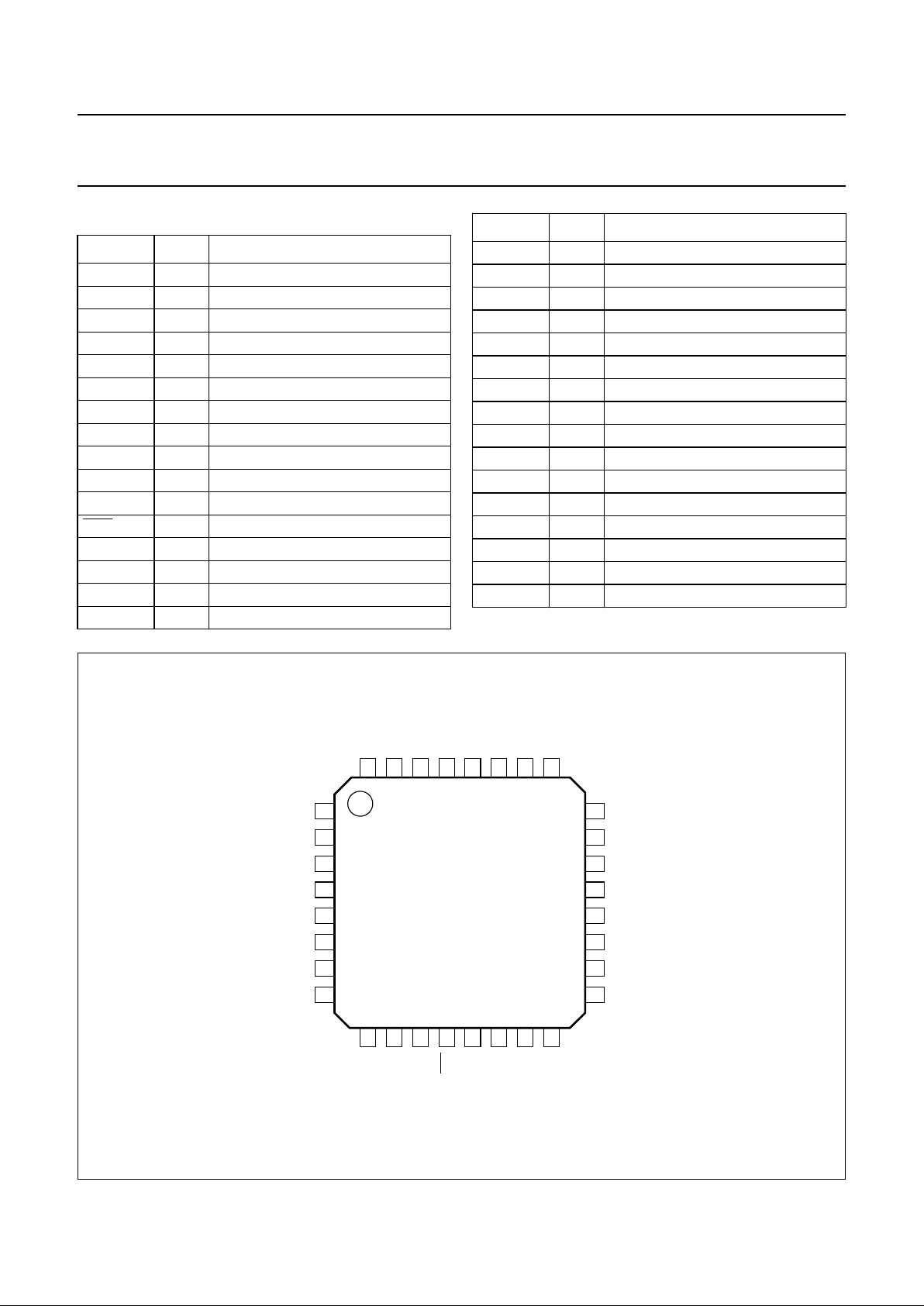
PINNING
SYMBOL PIN DESCRIPTION
n.c. 1 not connected
REFIN 2 reference input for ADC
INN 3 negative input
INP 4 positive input
REFOUT 5 reference for AC coupling
AGND 6 analog ground
V
CCA
7 analog supply voltage
STDBY 8 standby mode input
DGND 9 digital ground
V
CCD
10 digital supply voltage
CLK 11 clock input
TEN 12 track enable input (active LOW)
n.c. 13 not connected
n.c. 14 not connected
D0 15 data output bit 0 (LSB)
D1 16 data output bit 1
D2 17 data output bit 2
D3 18 data output bit 3
OGND1 19 output ground 1
V
CCO1
20 output supply voltage 1
OGND2 21 output ground 2
V
CCO2
22 output supply voltage 2
D4 23 data output bit 4
D5 24 data output bit 5
D6 25 data output bit 6
D7 26 data output bit 7 (MSB)
n.c 27 not connected
n.c 28 not connected
n.c 29 not connected
n.c 30 not connected
DEC 31 decoupling
SDN 32 stabilized decoupling node
SYMBOL PIN DESCRIPTION
handbook, full pagewidth
TDA8793
MGR017
1
2
3
4
5
6
7
8
24
23
22
21
20
19
18
17
9
10
11
12
13
14
15
16
32
31
30
29
28
27
26
25
n.c.
REFOUT
STDBY
V
CCA
INN
AGND
DGND
CLK
n.c.
V
CCD
D0
D7
n.c.
SDN
n.c.
V
CCO2
V
CCO1
n.c.
D4
D3
D2
OGND2
DEC
n.c.
D1
D6
D5
OGND1
n.c.
TEN
INP
REFIN
Fig.2 Pin configuration.
1999 Oct 06 5
Philips Semiconductors Preliminary specification
8-bit, low-power, 3 V, 100 Msps
Analog-to-Digital Converter (ADC)
TDA8793
LIMITING VALUES
In accordance with the Absolute Maximum Rating System (IEC 134).
HANDLING
Inputs and outputs are protected against electrostatic discharges in normal handling. However, to be totally safe, it is
desirable to take normal precautions appropriate to handling integrated circuits.
THERMAL CHARACTERISTICS
SYMBOL PARAMETER CONDITIONS MIN. MAX. UNIT
V
CCA
analog supply voltage −0.3 +7.0 V
V
CCD
digital supply voltage −0.3 +7.0 V
V
CCO
output stages supply voltage −0.3 +7.0 V
∆V
CC
supply voltage differences between
V
CCA
and V
CCD
−1.0 +1.0 V
V
CCO
and V
CCD
−1.0 +1.0 V
V
CCA
and V
CCO
−1.0 +1.0 V
V
INP, INN
input voltage range referenced to AGND −0.3 +7.0 V
I
O
output current − 10 mA
T
stg
storage temperature −55 +150 °C
T
amb
ambient temperature 0 70 °C
T
j
junction temperature −−°C
SYMBOL PARAMETER CONDITIONS VALUE UNIT
R
th(j-a)
thermal resistance from junction to ambient in free air 94 K/W
1999 Oct 06 6
Philips Semiconductors Preliminary specification
8-bit, low-power, 3 V, 100 Msps
Analog-to-Digital Converter (ADC)
TDA8793
CHARACTERISTICS
V
CCA=V7
to V6= 2.7 to 3.6 V; V
CCD=V10
to V9= 2.7 to 3.6 V; V
CCO=V20
(or V22) to V19 (or V21) = 2.7 to 3.6 V;
AGND to DGND and OGND shorted together; V
CCA
to V
CCD
= −0.15 to +0.15 V; V
CCD
to V
CCO
= −0.15 to +0.15 V;
V
CCA
to V
CCO
= −0.15 to +0.15 V; T
amb
= 0 to 70 °C; typical values measured at V
CCA=VCCD=VCCO
= 3.0 V and
T
amb
=25°C; single-ended input; unless otherwise specified.
SYMBOL PARAMETER CONDITIONS MIN. TYP. MAX. UNIT
Supplies
V
CCA
analog supply voltage 2.7 3.0 3.6 V
V
CCD
digital supply voltage 2.7 3.0 3.6 V
V
CCO
output stages supply voltage 2.7 3.0 3.6 V
I
CCA
analog supply current 32 40 48 mA
I
CCD
digital supply current 13 16 22 mA
I
CCO
output stages supply current fi= ramp input − 0.1 tbf mA
f
i
= 20 MHz − 4 tbf mA
Internal reference (pin SDN); note 1
V
ref
reference voltage 1.21 1.25 1.29 V
V
reg
line regulation voltage 2.7 < V
CCA
< 3.6 V − 0.4 3 mV
TC temperature coefficient − 18 − ppm/K
I
L
load current −1 −−mA
Internal reference (pin REFOUT)
V
o(ref)
reference voltage 1.76 1.82 1.88 V
V
o(reg)
line regulation voltage 2.7 < V
CCA
< 3.6 V − 1.5 4 mV
TC temperature coefficient − 18 − ppm/K
I
L
load current −1 −−mA
Adjustable full scale input (pin REFIN); see Figs 3, 4, and 7
I
ref
input current V
REFIN
= 1.25 V −−0.87 − mA
Clock input (pin CLK); note 2
V
IL
LOW-level input voltage 0 − 0.8 V
V
IH
HIGH-level input voltage 2 − V
CCD
V
I
IL
LOW-level input current V
CLK
=0 −2 − +2 µA
I
IH
HIGH-level input current V
CLK=VCCD
−−5µA
t
r
clock rise time 0.75 − tbf ns
t
f
clock fall time 0.75 − tbf ns
Z
i
input impedance f
CLK
= 100 MHz − 32 − kΩ
C
i
input capacitance f
CLK
= 100 MHz − 2 − pF
Standby input (pin STDBY); see Table 1
V
IL
LOW-level input voltage 0 − 0.8 V
V
IH
HIGH-level input voltage 2 − V
CCD
V
I
IL
LOW-level input current V
STDBY
=0 −5 −−µA
I
IH
HIGH-level input current V
STDBY=VCCD
−−5µA
 Loading...