

Philips TDA8792M-C2-R1, TDA8792M-C2, TDA8792M-C1 Datasheet
DATA SH EET
Product specification
Supersedes data of 1995 Apr 26
File under Integrated Circuits, IC02
1996 Feb 21
INTEGRATED CIRCUITS
TDA8792
3.3 V, 25 MHz 8-bit
analog-to-digital converter (ADC)
1996 Feb 21 2
Philips Semiconductors Product specification
3.3 V, 25 MHz 8-bit
analog-to-digital converter (ADC)
TDA8792
FEATURES
• 8-bit resolution
• Sampling rate up to 25 MHz
• 30 MHz input signal bandwidth (full scale)
• High signal-to-noise ratio over a large analog input
frequency range (7.3 effective bits at 4.43 MHz
full-scale input at f
clk
= 25 MHz)
• CMOS compatible digital inputs
• External reference voltage regulator
• Power dissipation only 53 mW (typical)
• Standby mode (only 1.2 mW typical)
• Low analog input capacitance, no buffer amplifier
required
• No sample-and-hold circuit required.
APPLICATIONS
Analog-to-digital conversion for:
• General purpose
• Hand-held equipment
• Mobile telecommunication
• Instrumentation
• Video.
GENERAL DESCRIPTION
The TDA8792 is a 8-bit analog-to-digital converter (ADC)
for low-voltage, portable applications. It operates at 3.3 V
and converts the analog input signal into 8-bit
binary-coded digital words at a maximum sampling rate of
25 MHz. The output data is valid after a delay of 6 clock
cycles.
QUICK REFERENCE DATA
ORDERING INFORMATION
SYMBOL PARAMETER CONDITIONS MIN. TYP. MAX. UNIT
V
DDA
analog supply voltage 2.85 3.3 3.6 V
V
DDD
digital supply voltage 2.70 3.3 3.6 V
V
DDO
output stages supply voltage 2.5 3.3 3.6 V
I
DDA
analog supply current − 12 20 mA
I
DDD
digital supply current − 36mA
I
DDO
output stages supply current f
clk
= 25 MHz; CL= 15 pF;
ramp input
− 12mA
INL integral non-linearity f
clk
= 25 MHz; ramp input −±0.4 ±0.8 LSB
DNL differential non-linearity f
clk
= 25 MHz; ramp input −±0.3 ±0.75 LSB
f
clk(max)
maximum clock frequency 25 −−MHz
P
tot
total power dissipation f
clk
= 25 MHz; CL= 15 pF;
ramp input
− 53 100 mW
TYPE
NUMBER
PACKAGE
NAME DESCRIPTION VERSION
TDA8792M SSOP24 plastic shrink small outline package; 24 leads; body width 5.3 mm SOT340-1
1996 Feb 21 3
Philips Semiconductors Product specification
3.3 V, 25 MHz 8-bit
analog-to-digital converter (ADC)
TDA8792
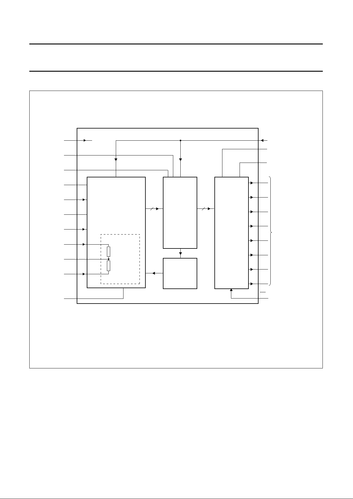
BLOCK DIAGRAM
Fig.1 Block diagram.
dbook, full pagewidth
1
2
3
4
5
6
7
8
8
9
10
12
V
DDO
V
SSO
STDBY
22
23
24
OUTPUT
BUFFER
DECODER
LATCHES
MLD119 - 1
D014
D1 15
D2 16
D317
D4 18
D519
D620
21 D7
OE 13
TDA8792
data outputs
LSB
MSB
DDD
V
SSD2
V
DDA
bias
V
RT
V
RM
V
RB
V
SSA2
V
SSA1
V
I
V
I
CLK
DAC
7 x 8
OFFSET
COMPENSATED
COMPARATORS
REFERENCE
LADDER
1996 Feb 21 4
Philips Semiconductors Product specification
3.3 V, 25 MHz 8-bit
analog-to-digital converter (ADC)
TDA8792
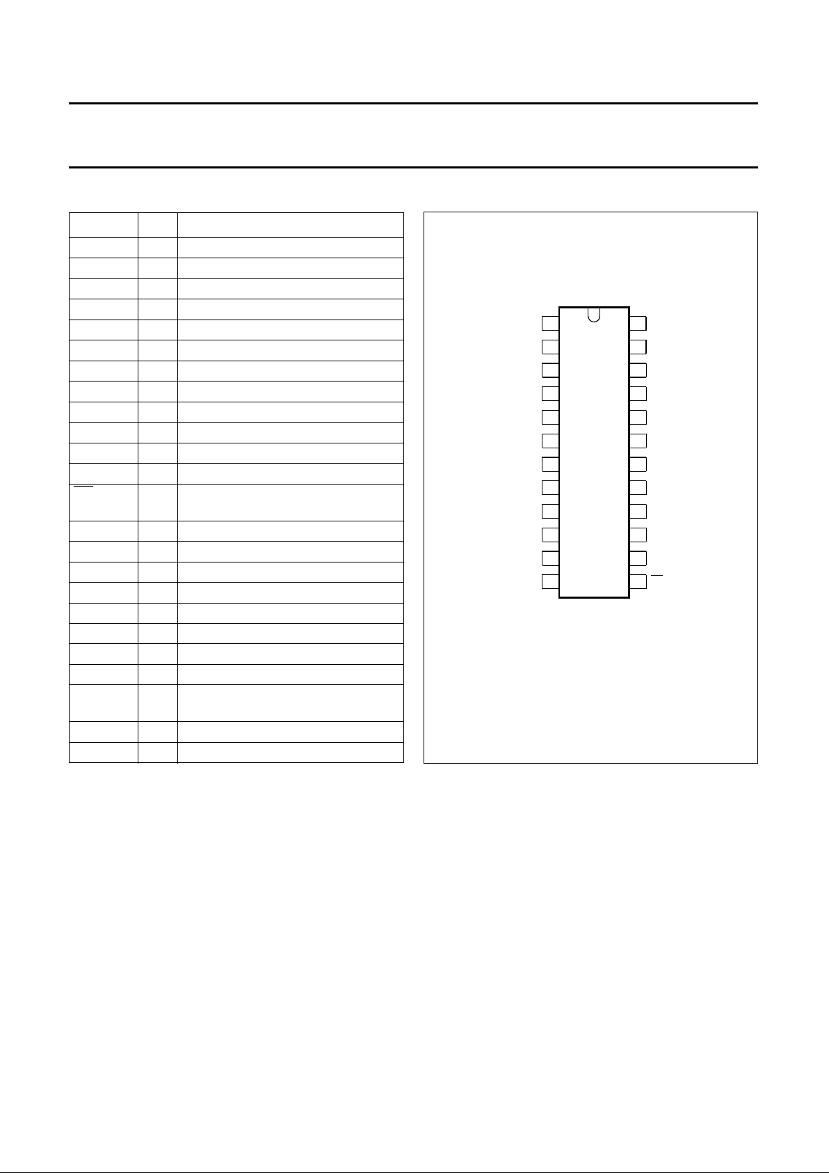
PINNING
SYMBOL PIN DESCRIPTION
STDBY 1 standby input
V
DDD
2 digital supply voltage (+3.3 V)
V
SSD2
3 digital ground 2
V
SSA1
4 analog ground 1
V
I
5 analog input voltage
V
DDA
6 analog supply voltage (+3.3 V)
I
bias
7 bias current input
V
RT
8 reference voltage TOP input
V
RM
9 reference voltage MIDDLE
V
RB
10 reference voltage BOTTOM input
n.c. 11 not connected
V
SSA2
12 analog ground 2
OE
13
output enable input (CMOS level
input, active LOW)
D0 14 data output; bit 0 (LSB)
D1 15 data output; bit 1
D2 16 data output; bit 2
D3 17 data output; bit 3
D4 18 data output; bit 4
D5 19 data output; bit 5
D6 20 data output; bit 6
D7 21 data output; bit 7 (MSB)
V
DDO
22
positive supply voltage for output
stage (+3.3 V)
V
SSO
23 output ground
CLK 24 clock input
Fig.2 Pin configuration.
handbook, halfpage
1
2
3
4
5
6
7
8
9
10
11
12
24
23
22
21
20
19
18
17
16
15
14
13
TDA8792
CLK
V
STDBY
V
n.c.
D1
D7
D6
D5
D4
D3
D2
D0
OE
V
I
bias
V
RM
V
RB
MLD120 - 1
V
RT
DDD
V
SSD2
V
SSA1
V
SSA2
V
DDA
V
I
SSO
DDO
1996 Feb 21 5
Philips Semiconductors Product specification
3.3 V, 25 MHz 8-bit
analog-to-digital converter (ADC)
TDA8792
LIMITING VALUES
In accordance with the Absolute Maximum Rating System (IEC 134).
Note
1. The supply voltages V
DDA
, V
DDD
and V
DDO
may have any value between −0.5 V and +5.0 V provided that the
differences ∆V
DD1
, ∆V
DD2
and ∆V
DD3
are respected.
HANDLING
Inputs and outputs are protected against electrostatic discharges in normal handling. However, to be totally safe, it is
desirable to take normal precautions appropriate to handling integrated circuits.
THERMAL CHARACTERISTICS
SYMBOL PARAMETER CONDITIONS MIN. MAX. UNIT
V
DDA
analog supply voltage note 1 −0.5 +5.0 V
V
DDD
digital supply voltage note 1 −0.5 +5.0 V
V
DDO
output stages supply voltage note 1 −0.5 +5.0 V
∆V
DD1
supply voltage differences between
∆V
DD1=VDDA
− V
DDD
−0.3 +0.3 V
∆V
DD2
supply voltage differences between
∆V
DD2=VDDD
− V
DDO
−1.0 +1.0 V
∆V
DD3
supply voltage differences between
∆V
DD3=VDDA
− V
DDO
−1.0 +1.0 V
V
I
input voltage referenced to V
SSA
−0.5 +5.0 V
V
clk(p-p)
AC input voltage for switching
(peak-to-peak value)
referenced to V
SSD
− V
DDD
V
I
O
output current − 10 mA
T
stg
storage temperature −55 +150 °C
T
amb
operating ambient temperature −20 +75 °C
T
j
junction temperature − +125 °C
SYMBOL PARAMETER VALUE UNIT
R
th j-a
thermal resistance from junction to ambient in free air 119 K/W
1996 Feb 21 6
Philips Semiconductors Product specification
3.3 V, 25 MHz 8-bit
analog-to-digital converter (ADC)
TDA8792
CHARACTERISTICS
V
DDA=V6
to V
4,12
= 2.85 to 3.6 V; V
DDD=V2
to V3and V1= 2.7 to 3.6 V; V
DDO=V22
to V23= 2.5 to 3.6 V;
V
SSA,VSSD
and V
SSO
shorted together; V
DDA
to V
DDD
= −0.15 to +0.15 V; f
clk
= 25 MHz; 50% duty factor; VIL=0V;
VIH=V
DDD
; CL= 15 pF; T
amb
= 0 to +70 °C; typical values measured at V
DDA=VDDD=VDDO
= 3.3 V and T
amb
=25°C;
unless otherwise specified.
SYMBOL PARAMETER CONDITIONS MIN. TYP. MAX. UNIT
Supply
V
DDA
analog supply voltage 2.85 3.3 3.6 V
V
DDD
digital supply voltage 2.7 3.3 3.6 V
V
DDO
output stages supply voltage 2.5 3.3 3.6 V
I
DDA
analog supply current − 12 20 mA
I
DDD
digital supply current − 36mA
I
DDO
output stages supply current CL= 15 pF; ramp input − 12mA
Inputs
C
LOCK INPUT CLK (REFERENCED TO V
SSD
); note 1
V
IL
LOW level input voltage 0 − 0.8 V
V
IH
HIGH level input voltage 2.0 − V
DDD
V
I
IL
LOW level input current V
clk
= 0.4 V −10 −−µA
I
IH
HIGH level input current V
clk
= 2.7 V −−10 µA
C
I
input capacitance − 10 − pF
INPUTS OE AND STDBY (REFERENCED TO V
SSD
); see Tables 2 and 3
V
IL
LOW level input voltage 0 − 0.8 V
V
IH
HIGH level input voltage 2.0 − V
DDD
V
I
IL
LOW level input current VIL= 0.4 V −10 −−µA
I
IH
HIGH level input current VIH= 2.7 V −−+10 µA
VI(ANALOG INPUT VOLTAGE REFERENCED TO V
SSA
)
I
IL
LOW level input current VI=0V −20 −−µA
I
IH
HIGH level input current VI= 1.5 V −−+20 µA
Z
I
input impedance fi= 4.43 MHz − 35 − kΩ
C
I
input capacitance fi= 4.43 MHz − 5 − pF
Reference voltages for the resistor ladder; see Table 1
V
RB
reference voltage BOTTOM 0 − 0.15 V
V
RT
reference voltage TOP 1.4 − 1.6 V
V
diff
differential reference voltage VRT− V
RB
1.25 1.5 1.6 V
I
ref
reference current − 1.3 − mA
R
LAD
resistor ladder − 1250 −Ω
TC
RLAD
temperature coefficient of the resistor
ladder
− 1 −Ω/K
 Loading...