

Philips TDA8790M-C2, TDA8790M-C1 Datasheet

DATA SH EET
Product specification
Supersedes data of 1995 May 08
File under Integrated Circuits, IC02
1996 Feb 21
INTEGRATED CIRCUITS
TDA8790
8-bit, 40 Msps 2.7 to 5.5 V universal
analog-to-digital converter

1996 Feb 21 2
Philips Semiconductors Product specification
8-bit, 40 Msps 2.7 to 5.5 V universal
analog-to-digital converter
TDA8790
FEATURES
• 8-bit resolution
• Operation between 2.7 and 5.5 V
• Sampling rate up to 40 MHz
• DC sampling allowed
• High signal-to-noise ratio over a large analog input
frequency range (7.3 effective bits at 4.43 MHz
full-scale input at f
clk
= 40 MHz)
• CMOS/TTL compatible digital inputs and outputs
• External reference voltage regulator
• Power dissipation only 30 mW (typical)
• Low analog input capacitance, no buffer amplifier
required
• Sleep mode (4 mW)
• No sample-and-hold circuit required.
APPLICATIONS
High-speed analog-to-digital conversion for:
• Video data digitizing
• Camera
• Camcorder
• Radio communication.
GENERAL DESCRIPTION
The TDA8790 is an 8-bit universal analog-to-digital
converter (ADC) for video and general purpose
applications. It converts the analog input signal from
2.7 to 5.5 V into 8-bit binary-coded digital words at a
maximum sampling rate of 40 MHz. All digital inputs and
outputs are CMOS/TTL compatible. A sleep mode allows
reduction of the device power consumption down to 4 mW.
QUICK REFERENCE DATA
ORDERING INFORMATION
SYMBOL PARAMETER CONDITIONS MIN. TYP. MAX. UNIT
V
DDA
analog supply voltage 2.7 3.3 5.5 V
V
DDD
digital supply voltage 2.7 3.3 5.5 V
V
DDO
output stages supply voltage 2.5 3.3 5.5 V
∆V
DD
supply voltage difference
V
DDA
− V
DDD
−0.2 − +0.2 V
V
DDD
− V
DDO
−0.2 − +2.25 V
I
DDA
analog supply current − 46mA
I
DDD
digital supply current − 58mA
I
DDO
output stages supply current f
clk
= 40 MHz; CL= 20 pF;
ramp input
− 12mA
INL integral non-linearity f
clk
= 40 MHz; ramp input −±0.5 ±0.75 LSB
DNL differential non-linearity f
clk
= 40 MHz; ramp input −±0.25 ±0.5 LSB
f
clk(max)
maximum clock frequency 40 −−MHz
P
tot
total power dissipation V
DDA=VDDD=VDDO
= 3.3 V − 30 53 mW
TYPE
NUMBER
PACKAGE
NAME DESCRIPTION VERSION
TDA8790M SSOP20 plastic shrink small outline package; 20 leads; body width 4.4 mm SOT266-1

1996 Feb 21 3
Philips Semiconductors Product specification
8-bit, 40 Msps 2.7 to 5.5 V universal
analog-to-digital converter
TDA8790
BLOCK DIAGRAM
Fig.1 Block diagram.
handbook, full pagewidth
7
9
8
10
V
RB
V
SSA
V
SSOVSSD1
V
RM
V
RT
V
R
LAD
I
3
V
DDD
5
V
DDA
17
18
19
16 D4
D5
D6
D7
15
14
2
D3
D2
13 D1
12
D0
CMOS
OUTPUTS
LATCHES
ANALOG -TO - DIGITAL
CONVERTER
CLOCK DRIVER
MBE502
1
CLK
SLEEP
TDA8790
20
V
DDO
6
analog
ground
411
output
ground
digital
ground
analog
voltage input
data outputs
LSB
MSB
1996 Feb 21 4
Philips Semiconductors Product specification
8-bit, 40 Msps 2.7 to 5.5 V universal
analog-to-digital converter
TDA8790
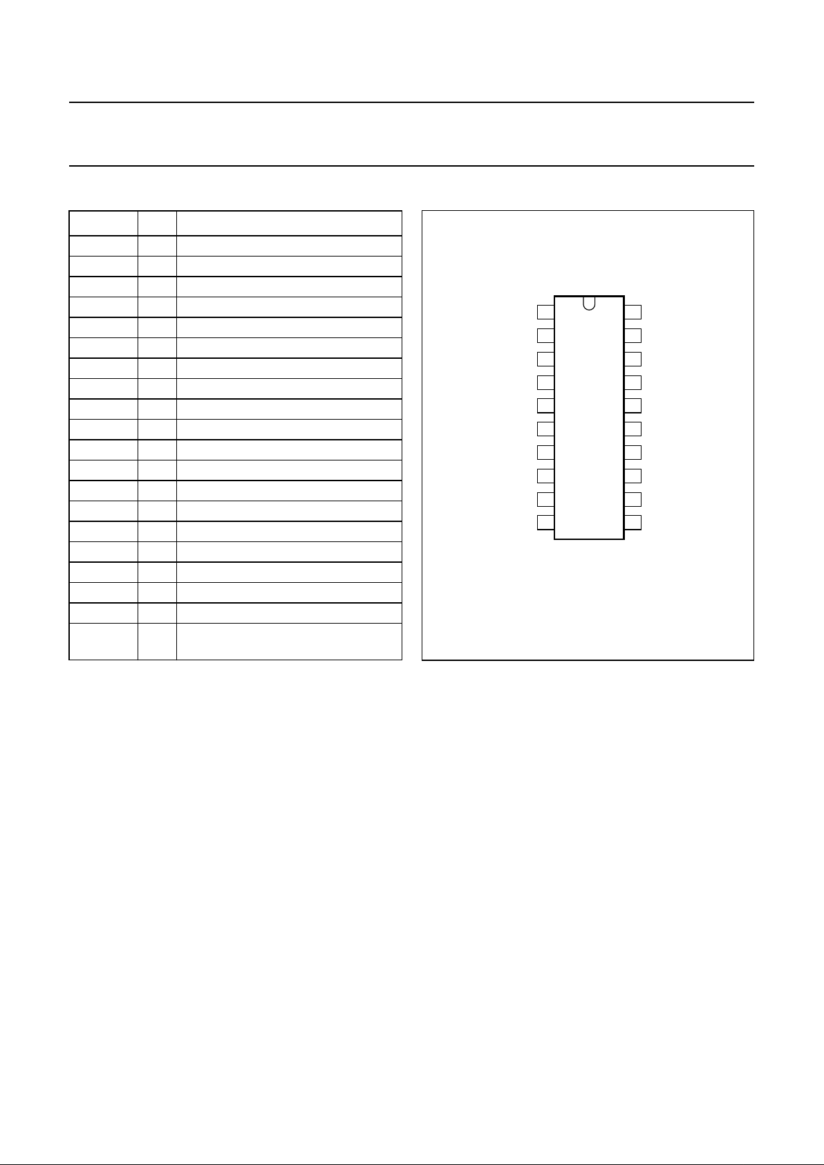
PINNING
SYMBOL PIN DESCRIPTION
CLK 1 clock input
SLEEP 2 sleep mode input
V
DDD
3 digital supply voltage (2.7 to 5.5 V)
V
SSD
4 digital ground
V
DDA
5 analog supply voltage (2.7 to 5.5 V)
V
SSA
6 analog ground
V
RB
7 reference voltage BOTTOM input
V
RM
8 reference voltage MIDDLE
V
I
9 analog input voltage
V
RT
10 reference voltage TOP input
V
SSO
11 digital output ground
D0 12 data output; bit 0 (LSB)
D1 13 data output; bit 1
D2 14 data output; bit 2
D3 15 data output; bit 3
D4 16 data output; bit 4
D5 17 data output; bit 5
D6 18 data output; bit 6
D7 19 data output; bit 7 (MSB)
V
DDO
20 positive supply voltage for output
stage (2.7 to 5.5 V)
Fig.2 Pin configuration.
TDA8790
MBE501
1
2
3
4
5
6
7
8
9
10
20
19
18
17
16
15
14
13
12
11
CLK
V
DDO
D7
D6
D5
D4
D3
D2
D1
D0
V
SSO
SLEEP
V
DDD
V
SSD
V
DDA
V
SSA
V
RB
V
RM
V
I
V
RT

1996 Feb 21 5
Philips Semiconductors Product specification
8-bit, 40 Msps 2.7 to 5.5 V universal
analog-to-digital converter
TDA8790
LIMITING VALUES
In accordance with the Absolute Maximum Rating System (IEC 134).
Note
1. The supply voltages V
DDA
, V
DDD
and V
DDO
may have any value between −0.3 V and +7.0 V provided that the supply
voltage ∆VDD remains as indicated.
HANDLING
Inputs and outputs are protected against electrostatic discharges in normal handling. However, to be totally safe, it is
desirable to take normal precautions appropriate to handling integrated circuits.
THERMAL CHARACTERISTICS
SYMBOL PARAMETER CONDITIONS MIN. MAX. UNIT
V
DDA
analog supply voltage note 1 −0.3 +7.0 V
V
DDD
digital supply voltage note 1 −0.3 +7.0 V
V
DDO
output stages supply voltage note 1 −0.3 +7.0 V
∆V
DD
supply voltage difference
V
DDA
− V
DDD
−1.0 +4.0 V
V
DDA
− V
DDO
−1.0 +4.0 V
V
DDD
− V
DDO
−1.0 +4.0 V
V
I
input voltage referenced to V
SSA
−0.3 +7.0 V
V
clk(p-p)
AC input voltage for switching
(peak-to-peak value)
referenced to V
SSD
− V
DDD
V
I
O
output current − 10 mA
T
stg
storage temperature −55 +150 °C
T
amb
operating ambient temperature −20 +75 °C
T
j
junction temperature − +150 °C
SYMBOL PARAMETER VALUE UNIT
R
th j-a
thermal resistance from junction to ambient in free air 120 K/W

1996 Feb 21 6
Philips Semiconductors Product specification
8-bit, 40 Msps 2.7 to 5.5 V universal
analog-to-digital converter
TDA8790
CHARACTERISTICS
V
DDA=V5
to V6= 3.3 V; V
DDD=V3
to V4= 3.3 V; V
DDO=V20
to V11= 3.3 V; V
SSA,VSSD
and V
SSO
shorted together;
V
i(p-p)
= 1.84 V; CL= 20 pF; T
amb
=0to+70°C; typical values measured at T
amb
=25°C; unless otherwise specified.
SYMBOL PARAMETER CONDITIONS MIN. TYP. MAX. UNIT
Supply
V
DDA
analog supply voltage 2.7 3.3 5.5 V
V
DDD
digital supply voltage 2.7 3.3 5.5 V
V
DDO
output stages supply voltage 2.5 3.3 5.5 V
∆V
DD
supply voltage difference
V
DDA
− V
DDD
−0.2 − +0.2 V
V
DDD
− V
DDO
−0.2 − +2.25 V
I
DDA
analog supply current − 46 mA
I
DDD
digital supply current − 58 mA
I
DDO
output stages supply current f
clk
= 40 MHz; ramp input;
CL=20pF
− 12 mA
Inputs
C
LOCK INPUT CLK (REFERENCED TO V
SSD
); see note 1
V
IL
LOW level input voltage 0 − 0.3V
DDD
V
V
IH
HIGH level input voltage 0.7V
DDD
− V
DDD
V
V
DDD
≤ 3.6 V 0.6V
DDD
− V
DDD
V
I
IL
LOW level input current V
clk
= 0.3V
DDD
−10+1µA
I
IH
HIGH level input current V
clk
= 0.7V
DDD
−−5µA
Z
I
input impedance f
clk
= 40 MHz − 4 − kΩ
C
I
input capacitance f
clk
= 40 MHz − 3 − pF
INPUT SLEEP (REFERENCED TO V
SSD
); see Table 2
V
IL
LOW level input voltage 0 − 0.3V
DDD
V
V
IH
HIGH level input voltage 0.7V
DDD
− V
DDD
V
V
DDD
≤ 3.6 V 0.6V
DDD
− V
DDD
V
I
IL
LOW level input current VIL= 0.3V
DDD
−1 −− µA
I
IH
HIGH level input current VIH= 0.7V
DDD
−−+1 µA
VI(ANALOG INPUT VOLTAGE REFERENCED TO V
SSA
)
I
IL
LOW level input current VI=V
RB
− 0 −µA
I
IH
HIGH level input current VI=V
RT
− 9 −µA
Z
I
input impedance fi= 1 MHz − 20 − kΩ
C
I
input capacitance fi= 1 MHz − 2 − pF
Reference voltages for the resistor ladder; see Table 1
V
RB
reference voltage BOTTOM 1.1 1.2 − V
V
RT
reference voltage TOP V
TOP
≤ V
DDA
2.7 3.3 V
DDA
V
V
diff
differential reference voltage
VRT− V
RB
1.5 2.1 2.7 V
I
ref
reference current − 0.95 − mA
 Loading...