

Philips TDA8714T-7-C1-R1, TDA8714T-7-C1, TDA8714T-6-C1, TDA8714T-6-C1-S1, TDA8714U-C1 Datasheet
...
DATA SH EET
Product specification
Supersedes data of 1996 Jan 31
File under Integrated Circuits, IC02
1997 Oct 29
INTEGRATED CIRCUITS
TDA8714
8-bit high-speed analog-to-digital
converter
1997 Oct 29 2
Philips Semiconductors Product specification
8-bit high-speed analog-to-digital converter TDA8714
FEATURES
• 8-bit resolution
• Sampling rate up to 80 MHz
• No missing codes guaranteed
• High signal-to-noise ratio over a large analog input
frequency range (7.7 effective bits at 4.43 MHz
full-scale input at f
clk
= 80 MHz)
• Overflow/underflow 3-state TTL output
• TTL compatible digital inputs
• Low-level AC clock input signal allowed
• External reference voltage regulator
• Power dissipation only 340 mW (typical)
• Low analog input capacitance, no buffer amplifier
required
• No sample-and-hold circuit required.
APPLICATIONS
High-speed analog-to-digital conversion for:
• video data digitizing
• radar pulse analysis
• transient signal analysis
• high energy physics research
•Σ∆ modulators
• medical imaging.
GENERAL DESCRIPTION
The TDA8714 is an 8-bit high-speed Analog-to-Digital
Converter (ADC) for professional video and other
applications. It converts the analog input signal into 8-bit
binary-coded digital words at a maximum sampling rate of
80 MHz. All digital inputs and outputs are TTL compatible,
although a low-level sine wave clock input signal is
allowed.
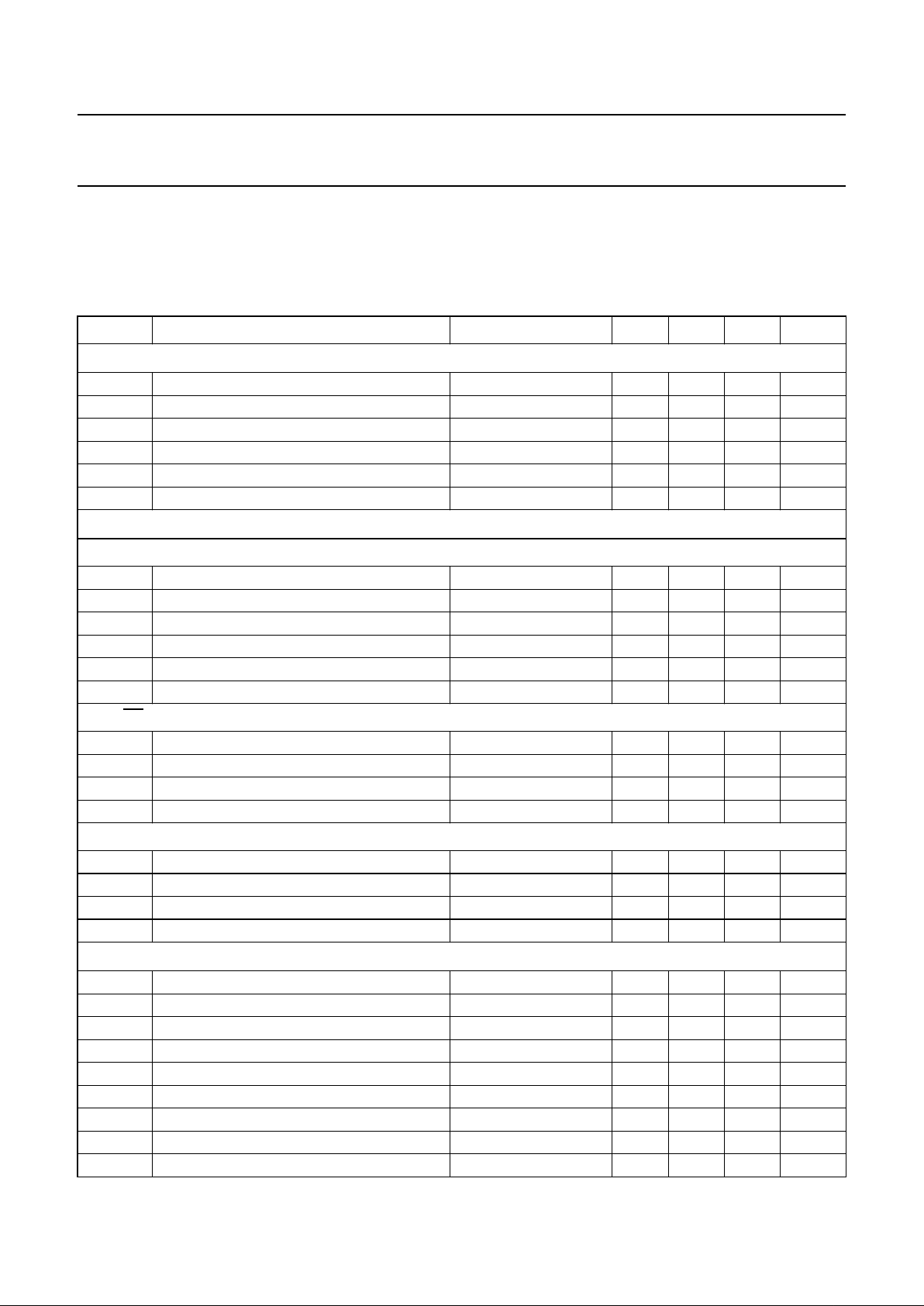
QUICK REFERENCE DATA
Note
1. Full-scale sine wave (f
i
= 4.43 MHz; f
clk
= 80 MHz).
SYMBOL PARAMETER CONDITIONS MIN. TYP. MAX. UNIT
V
CCA
analog supply voltage 4.75 5.0 5.25 V
V
CCD
digital supply voltage 4.75 5.0 5.25 V
V
CCO
output stages supply voltage 4.75 5.0 5.25 V
I
CCA
analog supply current − 25 30 mA
I
CCD
digital supply current − 27 33 mA
I
CCO
output stages supply current − 16 20 mA
INL DC integral non-linearity −±0.4 ±0.5 LSB
DNL DC differential non-linearity −±0.2 ±0.35 LSB
AINL AC integral non-linearity note 1 −±0.5 ±1.0 LSB
f
clk(max)
maximum clock frequency
TDA8714/7 80 −−MHz
TDA8714/6 60 −−MHz
TDA8714/4 40 −−MHz
P
tot
total power dissipation − 340 435 mW
1997 Oct 29 3
Philips Semiconductors Product specification
8-bit high-speed analog-to-digital converter TDA8714
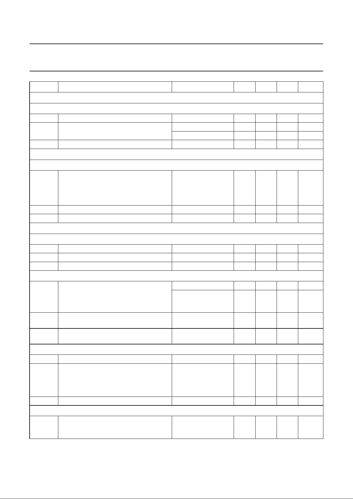
ORDERING INFORMATION
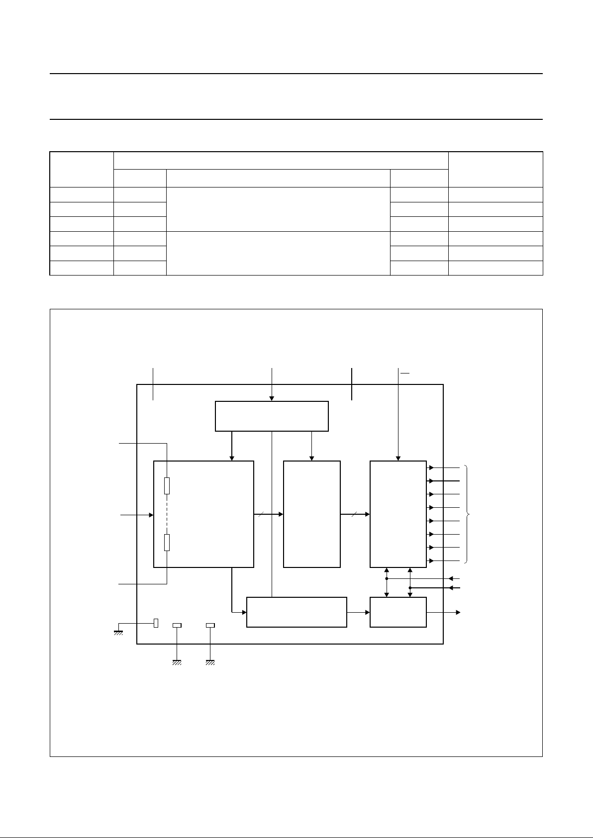
BLOCK DIAGRAM
TYPE
NUMBER
PACKAGE
SAMPLING
FREQUENCY (MHz)
NAME DESCRIPTION VERSION
TDA8714T/4 SO24 plastic small outline package; 24 leads;
body width 7.5 mm
SOT137-1 40
TDA8714T/6 SO24 SOT137-1 60
TDA8714T/7 SO24 SOT137-1 80
TDA8714M/4 SSOP24 plastic shrink small outline package; 24 leads;
body width 5.3 mm
SOT340-1 40
TDA8714M/6 SSOP24 SOT340-1 60
TDA8714M/7 SSOP24 SOT340-1 80
Fig.1 Block diagram.
handbook, full pagewidth
17
DGND
6
4
8
9
AGND
V
RB
V
RT
V
I
18
V
CCD
7
11
V
CCA
23
15
14
13
24 D2
D3
D4
D5
D6
1
2
12
D1
D0
D7
OVERFLOW / UNDERFLOW
LATCH
TTL OUTPUTSLATCHES
ANALOG -TO-DIGITAL
CONVERTER
CLOCK DRIVER
MSA669
TTL OUTPUT
16
CLK
22
CE
TDA8714
19
V
CCO1
analog ground digital ground
analog
voltage input
overflow / underflow
output
data outputs
LSB
MSB
21
V
CCO2
output ground
20
OGND
1997 Oct 29 4
Philips Semiconductors Product specification
8-bit high-speed analog-to-digital converter TDA8714
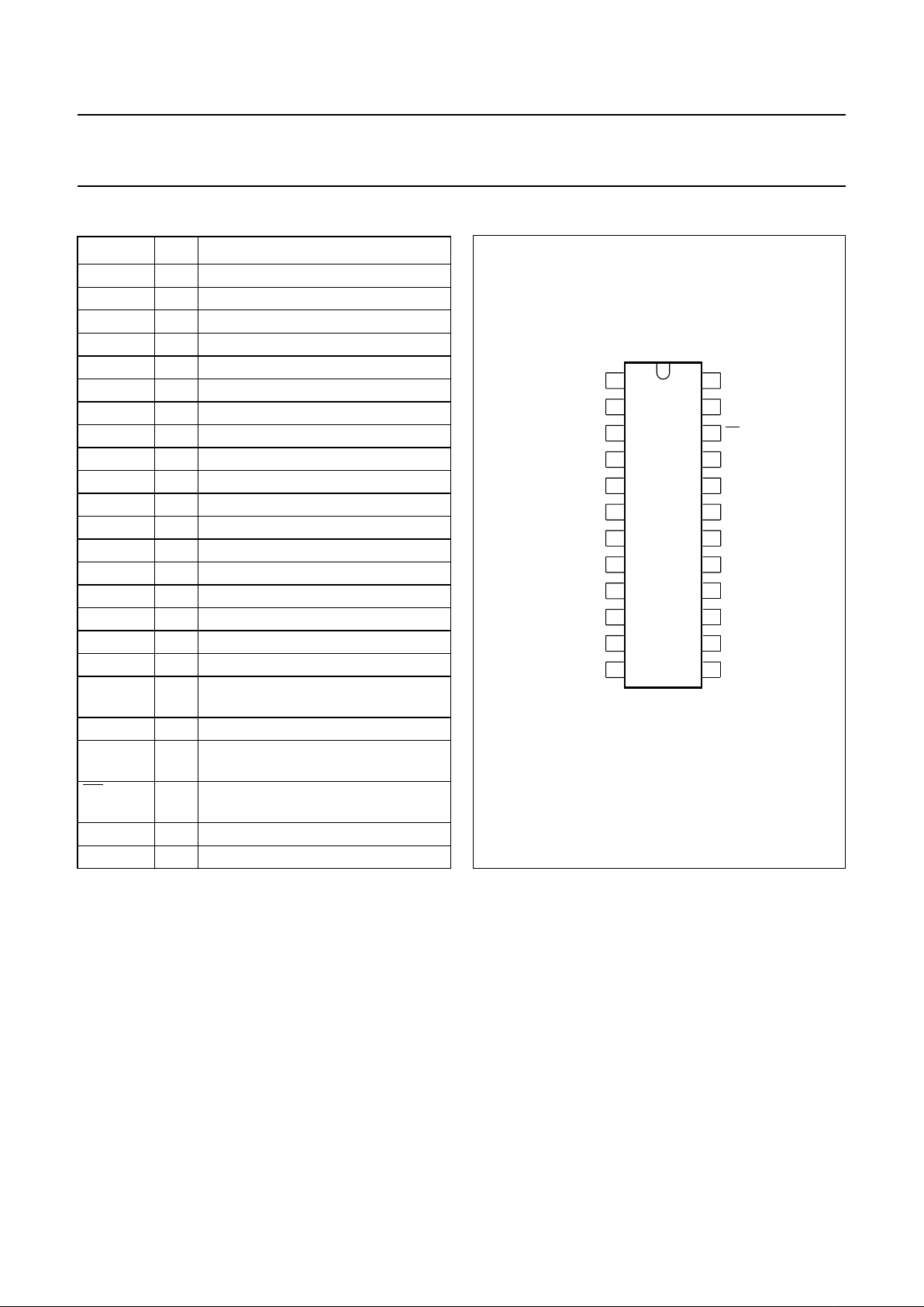
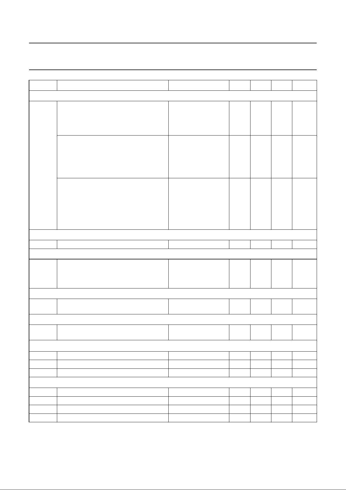
PINNING
SYMBOL PIN DESCRIPTION
D1 1 data output; bit 1
D0 2 data output; bit 0 (LSB)
n.c. 3 not connected
V
RB
4 reference voltage BOTTOM input
n.c. 5 not connected
AGND 6 analog ground
V
CCA
7 analog supply voltage (+5 V)
V
I
8 analog input voltage
V
RT
9 reference voltage TOP input
n.c. 10 not connected
O/UF 11 overflow/underflow data output
D7 12 data output; bit 7 (MSB)
D6 13 data output; bit 6
D5 14 data output; bit 5
D4 15 data output; bit 4
CLK 16 clock input
DGND 17 digital ground
V
CCD
18 digital supply voltage (+5 V)
V
CCO1
19 supply voltage for output stages 1
(+5 V)
OGND 20 output ground
V
CCO2
21 supply voltage for output stages 2
(+5 V)
CE 22 chip enable input (TTL level input,
active LOW)
D3 23 data output; bit 3
D2 24 data output; bit 2
Fig.2 Pin configuration.
handbook, halfpage
1
2
3
4
5
6
7
8
9
10
11
12
24
23
22
21
20
19
18
17
16
15
14
13
TDA8714
D2
D3
D1
D0
n.c.
O/UF
D7
V
CCO1
OGND
AGND
n.c.
V
RB
CLK
D4
D5
D6
DGND
CE
V
CCD
V
CCA
V
V
RT
n.c.
MSA667
CCO2
V
I
1997 Oct 29 5
Philips Semiconductors Product specification
8-bit high-speed analog-to-digital converter TDA8714
LIMITING VALUES
In accordance with the Absolute Maximum Rating System (IEC 134).
Note
1. The supply voltages V
CCA
and V
CCD
may have any value between −0.3 V and +7.0 V provided the difference
between V
CCA
and V
CCD
is between −1 V and +1 V.
HANDLING
Inputs and outputs are protected against electrostatic discharges in normal handling. However, to be totally safe, it is
desirable to take normal precautions appropriate to handling integrated circuits.
THERMAL CHARACTERISTICS
SYMBOL PARAMETER CONDITIONS MIN. MAX. UNIT
V
CCA
analog supply voltage note 1 −0.3 +7.0 V
V
CCD
digital supply voltage note 1 −0.3 +7.0 V
V
CCO
output stages supply voltage note 1 −0.3 +7.0 V
∆V
CC
supply voltage differences between
V
CCA
and V
CCD
−1.0 +1.0 V
∆V
CC
supply voltage differences between
V
CCO
and V
CCD
−1.0 +1.0 V
∆V
CC
supply voltage differences between
V
CCA
and V
CCO
−1.0 +1.0 V
V
I
input voltage referenced to AGND −0.3 +7.0 V
V
clk(p-p)
AC input voltage for switching
(peak-to-peak value)
referenced to DGND − V
CCD
V
I
O
output current − 10 mA
T
stg
storage temperature −55 +150 °C
T
amb
operating ambient temperature 0 +70 °C
T
j
junction temperature − +150 °C
SYMBOL PARAMETER VALUE UNIT
R
th j-a
thermal resistance from junction to ambient in free air
SOT137-1 75 K/W
SOT340-1 119 K/W
1997 Oct 29 6
Philips Semiconductors Product specification
8-bit high-speed analog-to-digital converter TDA8714
CHARACTERISTICS
V
CCA=V7
to V6= 4.75 to 5.25 V; V
CCD=V18
to V17= 4.75 to 5.25 V; V
CCO=V19
and V21to V20= 4.75 to 5.25 V;
AGND and DGND shorted together; V
CCA
to V
CCD
= −0.25 to +0.25 V; V
CCO
to V
CCD
= −0.25 to +0.25 V;
V
CCA
to V
CCO
= −0.25 to +0.25 V; V
i(p-p)
= 1.75 V; T
amb
= 0 to +70 °C; typical values measured at
V
CCA=VCCD=VCCO
= 5 V and T
amb
=25°C; unless otherwise specified.
SYMBOL PARAMETER CONDITIONS MIN. TYP. MAX. UNIT
Supply
V
CCA
analog supply voltage 4.75 5.0 5.25 V
V
CCD
digital supply voltage 4.75 5.0 5.25 V
V
CCO
output stages supply voltage 4.75 5.0 5.25 V
I
CCA
analog supply current − 25 30 mA
I
CCD
digital supply current − 27 33 mA
I
CCO
output stages supply current − 16 20 mA
Inputs
C
LOCK INPUT CLK (REFERENCED TO DGND); note 1
V
IL
LOW level input voltage 0 − 0.8 V
V
IH
HIGH level input voltage 2.0 − V
CCD
V
I
IL
LOW level input current V
clk
= 0.4 V −400 −−µA
I
IH
HIGH level input current V
clk
= 2.7 V −−300 µA
Z
I
input impedance f
clk
= 80 MHz − 18 − kΩ
C
I
input capacitance f
clk
= 80 MHz − 1 − pF
INPUT CE (REFERENCED TO DGND); see Table 2
V
IL
LOW level input voltage 0 − 0.8 V
V
IH
HIGH level input voltage 2.0 − V
CCD
V
I
IL
LOW level input current VIL= 0.4 V −400 −−µA
I
IH
HIGH level input current VIH= 2.7 V −−20 µA
VI(ANALOG INPUT VOLTAGE REFERENCED TO AGND)
I
IL
LOW level input current VI= 1.2 V − 0 −µA
I
IH
HIGH level input current VI= 3.5 V 60 130 280 µA
Z
I
input impedance fi= 4.43 MHz − 10 − kΩ
C
I
input capacitance fi= 4.43 MHz − 14 − pF
Reference voltages for the resistor ladder; see Table 1
V
RB
reference voltage BOTTOM 1.2 1.3 1.6 V
V
RT
reference voltage TOP 3.5 3.6 3.9 V
V
diff
differential reference voltage VRT− V
RB
1.9 2.3 2.7 V
I
ref
reference current − 11.5 − mA
R
LAD
resistor ladder − 200 −Ω
TC
RLAD
temperature coefficient of the resistor ladder − 0.24 − ppm
V
osB
offset voltage BOTTOM note 2 275 285 295 mV
V
osT
offset voltage TOP note 2 305 315 325 mV
V
i(p-p)
analog input voltage (peak-to-peak value) 1.45 1.75 2.15 V
1997 Oct 29 7
Philips Semiconductors Product specification
8-bit high-speed analog-to-digital converter TDA8714
Outputs
DIGITAL OUTPUTS D7 to D0 (REFERENCED TO DGND)
V
OL
LOW level output voltage IO= 1 mA 0 − 0.4 V
V
OH
HIGH level output voltage IO= −0.4 mA 2.7 − V
CCD
V
I
O
= −1 mA 2.4 − V
CCD
V
I
OZ
output current in 3-state mode 0.4V<VO<V
CCD
−20 − +20 µA
Switching characteristics
C
LOCK INPUT CLK (note 1; see Fig.3)
f
clk(max)
maximum clock frequency
TDA8714/4 40 −−MHz
TDA8714/6 60 −−MHz
TDA8714/7 80 −−MHz
t
CPH
clock pulse width HIGH 6 −−ns
t
CPL
clock pulse width LOW 6 −−ns
Analog signal processing
L
INEARITY
INL DC integral non-linearity −±0.4 ±0.5 LSB
DNL DC differential non-linearity −±0.2 ±0.35 LSB
AINL AC integral non-linearity note 3 −±0.5 ±1.0 LSB
B
ANDWIDTH (f
clk
= 40 MHz); note 4
B analog bandwidth full-scale sine wave − 13 − MHz
75% full-scale sine
wave; small signal at
Vi= ±5 LSB, code 128
− 20 − MHz
t
STLH
analog input settling time LOW-to-HIGH full-scale square
wave; Fig.6; note 5
− 2.5 3.5 ns
t
STHL
analog input settling time HIGH-to-LOW full-scale square
wave; Fig.6; note 5
− 3.0 4.0 ns
HARMONICS (f
clk
= 40 MHz)
h
1
fundamental harmonics (full scale) fi= 4.43 MHz −−0dB
h
all
harmonics (full scale);
all components
fi= 4.43 MHz
second harmonics −−64 −60 dB
third harmonics −−58 −55 dB
THD total harmonic distortion f
i
= 4.43 MHz −−56 − dB
SIGNAL-TO-NOISE RATIO (note 6; see Figs 7 and 13)
S/N signal-to-noise ratio (full scale) without harmonics;
f
clk
= 40 MHz;
fi= 4.43 MHz
46 48 − dB
SYMBOL PARAMETER CONDITIONS MIN. TYP. MAX. UNIT
1997 Oct 29 8
Philips Semiconductors Product specification
8-bit high-speed analog-to-digital converter TDA8714
EFFECTIVE BITS (note 6; see Figs 7 and 13)
EB effective bits
TDA8714/4 f
clk
= 40 MHz
f
i
= 4.43 MHz − 7.75 − bits
f
i
= 7.5 MHz − 7.6 − bits
effective bits
TDA8714/6 f
clk
= 60 MHz
f
i
= 4.43 MHz − 7.7 − bits
f
i
= 7.5 MHz − 7.55 − bits
f
i
= 10 MHz − 7.4 − bits
effective bits
TDA8714/7 f
clk
= 80 MHz
f
i
= 4.43 MHz − 7.7 − bits
f
i
= 7.5 MHz − 7.5 − bits
f
i
= 10 MHz − 7.2 − bits
f
i
= 15 MHz − 6.3 − bits
TWO-TONE (note 7)
TTIR two-tone intermodulation rejection f
clk
= 40 MHz −−56 − dB
BIT ERROR RATE
BER bit error rate f
clk
= 40 MHz;
fi= 4.43 MHz;
VI= ±16 LSB at
code 128
− 10
−11
− times/
samples
DIFFERENTIAL GAIN (note 8)
G
diff
differential gain f
clk
= 40 MHz;
fi= 4.43 MHz
− 0.6 − %
DIFFERENTIAL PHASE (note 8)
ϕ
diff
differential phase f
clk
= 40 MHz;
fi= 4.43 MHz
− 0.8 − deg
Timing (note 9; see Figs 3 and 5; f
clk
= 80 MHz)
t
ds
sampling delay time −−2ns
t
h
output hold time 5 −−ns
t
d
output delay time − 10 11 ns
3-state output delay times (see Fig.4)
t
dZH
enable HIGH − 40 44 ns
t
dZL
enable LOW − 12 16 ns
t
dHZ
disable HIGH − 50 54 ns
t
dLZ
disable LOW − 10 14 ns
SYMBOL PARAMETER CONDITIONS MIN. TYP. MAX. UNIT
 Loading...