


DATA SH EET
Product specification
Supersedes data of April 1993
File under Integrated Circuits, IC02
June 1994
INTEGRATED CIRCUITS
Philips Semiconductors
TDA8708A
Video analog input interface
June 1994 2
Philips Semiconductors Product specification
Video analog input interface TDA8708A
FEATURES
• 8-bit resolution
• Sampling rate up to 32 MHz
• Binary or two's complement 3-state TTL outputs
• TTL-compatible digital inputs and outputs
• Internal reference voltage regulator
• Power dissipation of 365 mW (typical)
• Input selector circuit (one out of three video inputs)
• Clamp and Automatic Gain Control (AGC) functions for
CVBS and Y signals
• No sample-and-hold circuit required.
• The TDA8708A has white peak control in modes 1 and
2 whereas the TDA8708B has control in mode 1 only.
APPLICATIONS
• Video signal decoding
• Scrambled TV (encoding and decoding)
• Digital picture processing
• Frame grabbing.
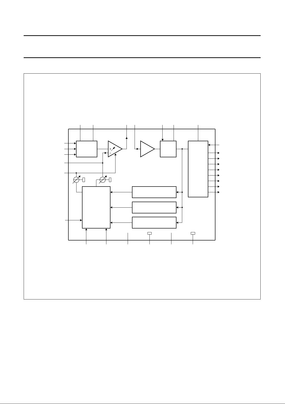
GENERAL DESCRIPTION
The TDA8708A is an analog input interface for video signal
processing. It includes a video amplifier with clamp and
gain control, an 8-bit analog-to-digital converter (ADC)
with a sampling rate of 32 MHz and an input selector.
QUICK REFERENCE DATA
ORDERING INFORMATION
SYMBOL PARAMETER MIN. TYP. MAX. UNIT
V
CCA
analog supply voltage 4.5 5.0 5.5 V
V
CCD
digital supply voltage 4.5 5.0 5.5 V
V
CCO
TTL output supply voltage 4.2 5.0 5.5 V
I
CCA
analog supply current − 37 45 mA
I
CCD
digital supply current − 24 30 mA
I
CCO
TTL output supply current − 12 16 mA
ILE DC integral linearity error −−±1 LSB
DLE DC differential linearity error −−±0.5 LSB
f
clk(max)
maximum clock frequency 30 32 − MHz
B maximum −3 dB bandwidth (AGC amplifier) 12 18 − MHz
P
tot
total power dissipation − 365 500 mW
TYPE NUMBER
PACKAGE
PINS PIN POSITION MATERIAL CODE
TDA8708A 28 DIP plastic SOT117-1
TDA8708AT 28 SO28L plastic SOT136-1
June 1994 3
Philips Semiconductors Product specification
Video analog input interface TDA8708A
BLOCK DIAGRAM
Fig.1 Block diagram.
ndbook, full pagewidth
MBB965
TTL
OUTPUTS
9
1
2
3
4
10
11
12
13
output format/
chip enable
(3-state input)
D7
D6
D5
D4
D3
D2
D1
D0
8 - bit
ADC
AMP.
VIDEO
AMPLIFIER
INPUT
SELECTOR
16
17
18
19 2014 15
video input
selection bit 0
video input
selection bit 1
analog
voltage
output
ADC
input
clock
input
decoupling
input
521 7
TTL outputs
video input 0
video input 1
video input 2
clamp capacitor
connection
AGC capacitor
connection
24
25
AGC &
CLAMP
LOGIC
&
MODE
SELECTION
PEAK LEVEL
DIGITAL COMPARATOR
27 26
sync level
sync pulse
black level
sync pulse
6
digital V
CCD
(+ 5 V)
digital
ground
8 22
analog V
CCA
(+ 5 V)
V
CCO
(+ 5 V)
analog
ground
23
TDA8708A
28
BLACK LEVEL
DIGITAL COMPARATOR
SYNC LEVEL
DIGITAL COMPARATOR
peak level current
resistor input
June 1994 4
Philips Semiconductors Product specification
Video analog input interface TDA8708A
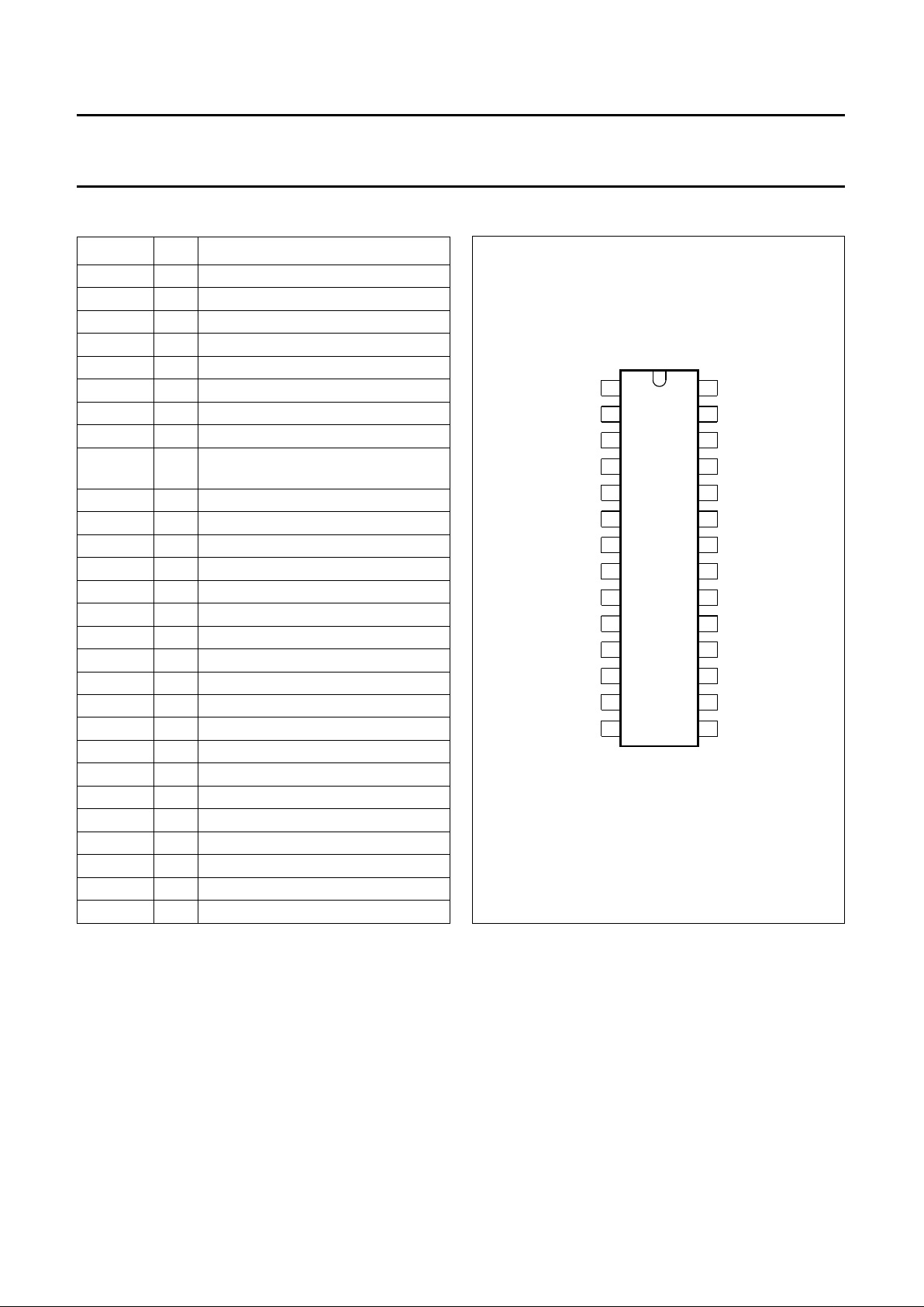
PINNING
SYMBOL PIN DESCRIPTION
D7 1 data output; bit 7 (MSB)
D6 2 data output; bit 6
D5 3 data output; bit 5
D4 4 data output; bit 4
CLK 5 clock input
V
CCD
6 digital supply voltage (+5 V)
V
CCO
7 TTL outputs supply voltage (+5 V)
DGND 8 digital ground
OF 9 output format/chip enable
(3-state input)
D3 10 data output; bit 3
D2 11 data output; bit 2
D1 12 data output; bit 1
D0 13 data output; bit 0 (LSB)
I0 14 video input selection bit 0
I1 15 video input selection bit 1
VIN0 16 video input 0
VIN1 17 video input 1
VIN2 18 video input 2
ANOUT 19 analog voltage output
ADCIN 20 analog-to-digital converter input
DEC 21 decoupling input
V
CCA
22 analog supply voltage (+5 V)
AGND 23 analog ground
CLAMP 24 clamp capacitor connection
AGC 25 AGC capacitor connection
GATE B 26 black level synchronization pulse
GATE A 27 sync level synchronization pulse
RPEAK 28 peak level current resistor input
Fig.2 Pin configuration.
1
2
3
4
5
6
7
8
9
10
11
12
13
28
27
26
25
24
23
22
21
20
19
18
17
16
1514
TDA8708A
D7
D6
D5
D4
CLK
V
CCD
V
CCO
DGND
OF
D3
D2
D1
D0
I0
ADCIN
ANOUT
VIN2
VIN1
VIN0
I1
GATE B
AGC
CLAMP
AGND
V
CCA
DEC
RPEAK
GATE A
MBB964
June 1994 5
Philips Semiconductors Product specification
Video analog input interface TDA8708A
FUNCTIONAL DESCRIPTION
The TDA8708A provides a simple interface for decoding
video signals.
The TDA8708A operates in configuration mode 1 (see
Fig.4) when the video signals are weak (i.e. when the gain
of the AGC amplifier has not yet reached its optimum
value). This enables a fast recovery of the synchronization
pulses in the decoder circuit. When the pulses at the
GATE A and GATE B inputs become distinct (GATE A and
GATE B pulses are synchronization pulses occurring
during the sync period and rear porch respectively) the
TDA8708A automatically switches to configuration mode 2
(see Fig.5).
When the TDA8708A is in configuration mode 1, the gain
of the AGC amplifier will be roughly adjusted (sync level to
a digital output level of 0 and the peak level to a digital
output level of 255).
In configuration mode 2 the digital output of the ADC is
compared to internal digital reference levels. The resultant
outputs control the charge or discharge current of a
capacitor connected to the AGC pin. The voltage across
this capacitor controls the gain of the video amplifier. This
is the gain control loop.
The sync level comparator is active during a positive-going
pulse at the GATE A input. This means that the sync pulse
of the composite video signal is used as an amplitude
reference. The bottom of the sync pulse is adjusted to
obtain a digital output of logic 0 at the converter output. As
the black level is at digital level 64, the sync pulse will have
a digital amplitude of 64 LSBs.
The peak-white control loop is always active. If the video
signal tends to exceed the digital code of 248, the gain will
be limited to avoid any over-range of the converter.
The use of nominal signals will prevent the output from
exceeding a digital code of 213 and the peak-white control
loop will be non-active.
The clamp level control is accomplished by using the same
techniques as used for the gain control. The black-level
digital comparator is active during a positive-going pulse at
the GATE B input. The clamp capacitor will be charged or
discharged to adjust the digital output to code 64.
LIMITING VALUES
In accordance with the Absolute Maximum Rating System (IEC 134).
THERMAL CHARACTERISTICS
SYMBOL PARAMETER MIN. MAX. UNIT
V
CCA
analog supply voltage −0.3 +7.0 V
V
CCD
digital supply voltage −0.3 +7.0 V
V
CCO
output supply voltage −0.3 +7.0 V
∆V
CC
supply voltage difference between V
CCA
and V
CCD
−1.0 +1.0 V
supply voltage difference between V
CCO
and V
CCD
−1.0 +1.0 V
supply voltage difference between V
CCA
and V
CCO
−1.0 +1.0 V
V
I
input voltage −0.3 V
CCA
V
I
O
output current 0 +10 mA
T
stg
storage temperature −55 +150 °C
T
amb
operating ambient temperature 0 +70 °C
T
j
junction temperature 0 +125 °C
SYMBOL PARAMETER VALUE UNIT
R
th j-a
thermal resistance from junction to ambient in free air
SOT117-1 55 K/W
SOT136-1 70 K/W
June 1994 6
Philips Semiconductors Product specification
Video analog input interface TDA8708A
CHARACTERISTICS
V
CCA
= V22to V23 = 4.5 to 5.5 V; V
CCD
= V6to V8 = 4.5 to 5.5 V; V
CCO
= V7to V8 = 4.2 to 5.5 V; AGND and DGND
shorted together; V
CCA
to V
CCD
= −0.5 to +0.5 V; V
CCO
to V
CCD
= −0.5 to +0.5 V; V
CCA
to V
CCO
= −0.5 to +0.5 V;
T
amb
= 0 to +70 °C; typical readings taken at V
CCA
= V
CCD
= V
CCO
= 5 V and T
amb
= 25 °C; unless otherwise specified.
SYMBOL PARAMETER CONDITIONS MIN. TYP. MAX. UNIT
Supplies
V
CCA
analog supply voltage 4.5 5.0 5.5 V
V
CCD
digital supply voltage 4.5 5.0 5.5 V
V
CCO
TTL output supply voltage 4.2 5.0 5.5 V
I
CCA
analog supply current − 37 45 mA
I
CCD
digital supply current − 24 30 mA
I
CCO
TTL output supply current TTL load (see Fig.8) − 12 16 mA
Video amplifier inputs
VIN(0
TO 2) INPUTS
V
I(p-p)
input voltage (peak-to-peak value) AGC load with external
capacitor; note 1
0.6 − 1.5 V
|Z
i
| input impedance fi= 6 MHz 10 20 − kΩ
C
I
input capacitance fi = 6 MHz − 1 − pF
I0 AND I1 TTL INPUTS (SEE TABLE 1)
V
IL
LOW level input voltage 0 − 0.8 V
V
IH
HIGH level input voltage 2.0 − V
CCD
V
I
IL
LOW level input current VI = 0.4 V −400 −−µA
I
IH
HIGH level input current VI = 2.7 V −− 20 µA
GATE A AND GATE B TTL INPUTS (SEE FIGS 4 AND 5)
V
IL
LOW level input voltage 0 − 0.8 V
V
IH
HIGH level input voltage 2.0 − V
CCD
V
I
IL
LOW level input current VI = 0.4 V −400 −−µA
I
IH
HIGH level input current VI = 2.7 V −− 20 µA
t
W
pulse width see Fig.5 2 −−µs
RPEAK INPUT (PIN 28)
I
28(min)
minimum peak level current R28 = 0 Ω−80 150 µA
AGC INPUT (PIN 25)
V
25(min)
AGC voltage for minimum gain − 2.8 − V
V
25(max)
AGC voltage for maximum gain − 4.0 − V
AGC output current see Table 2
CLAMP
INPUT (PIN 24)
V
24
clamp voltage for code 128 output − 3.5 − V
I
24
clamp output current see Table 3
June 1994 7
Philips Semiconductors Product specification
Video analog input interface TDA8708A
Video amplifier outputs
ANOUT OUTPUT (PIN 19)
V
19(p-p)
AC output voltage
(peak-to-peak value)
V
VIN
= 1.33 V (p-p);
V25= 3.6 V
− 1.33 − V
I
19
internal current source RL = ∞ 2.0 2.5 − mA
I
O(p-p)
output current driven by the load V
ANOUT
= 1.33 V (p-p);
note 2
−− 1.0 mA
V
19
DC output voltage for black level note 3 − V
CCA
− 2.24 − V
Z
19
output impedance − 20 −Ω
Video amplifier dynamic characteristics
α
ct
crosstalk between VIN inputs V
CCA
= 4.75 to 5.25 V −−50 −45 dB
G
diff
differential gain V
VIN
= 1.33 V (p-p);
V25= 3.6 V
− 2 − %
ϕ
diff
differential phase V
VIN
= 1.33 V (p-p);
V25= 3.6 V
− 0.8 − deg
B −3 dB bandwidth 12 −−MHz
S/N signal-to-noise ratio note 4 60 −−dB
SVRR1 supply voltage ripple rejection note 5 − 45 − dB
∆G gain range see Fig.10 −4.5 − +6.0 dB
G
stab
gain stability as a function of supply
voltage and temperature
see Fig.10 −− 5%
Analog-to-digital converter inputs
CLK
INPUT (PIN 5)
V
IL
LOW level input voltage 0 − 0.8 V
V
IH
HIGH level input voltage 2.0 − V
CCD
V
I
IL
LOW level input current V
clk
= 0.4 V −400 −−µA
I
IH
HIGH level input current V
clk
= 2.7 V −− 100 µA
|Z
i
| input impedance f
clk
= 10 MHz − 4 − kΩ
C
I
input capacitance f
clk
= 10 MHz − 4.5 − pF
OF INPUT (3-STATE; SEE TABLE 4)
V
IL
LOW level input voltage 0 − 0.2 V
V
IH
HIGH level input voltage 2.6 − V
CCD
V
V
9
input voltage in high impedance state − 1.15 − V
I
IL
LOW level input current −370 −300 −µA
I
IH
HIGH level input current − 300 450 µA
SYMBOL PARAMETER CONDITIONS MIN. TYP. MAX. UNIT
June 1994 8
Philips Semiconductors Product specification
Video analog input interface TDA8708A
ADCIN INPUT (PIN 20; SEE TABLE 5)
V
20
input voltage digital output = 00 − V
CCA
− 2.42 − V
V
20
input voltage digital output = 255 − V
CCA
− 1.41 − V
V
20(p-p)
input voltage amplitude
(peak-to-peak value)
− 1.0 − V
I
20
input current − 1.0 10 µA
|Z
i
| input impedance fi= 6 MHz − 50 − MΩ
C
I
input capacitance fi = 6 MHz − 1 − pF
Analog-to-digital converter outputs
D
IGITAL OUTPUTS D0 TO D7
V
OL
LOW level output voltage IOL = 2 mA 0 − 0.6 V
V
OH
HIGH level output voltage IOL = −0.4 mA 2.4 − V
CCD
V
I
OZ
output current in 3-state mode 0.4 V < VO< V
CCD
−20 − +20 µA
Switching characteristics
f
clk(max)
maximum clock input frequency see Fig.6; note 6 30 32 − MHz
Analog signal processing (f
clk
= 32 MHz; see Fig.8)
G
diff
differential gain V20 = 1.0 V (p-p);
see Fig.3; note 7
− 2 − %
ϕ
diff
differential phase see Fig.3; note 7 − 2 − deg
f
1
fundamental harmonics (full-scale) fi= 4.43 MHz; note 7 −− 0dB
f
all
harmonics (full-scale);
all components
fi= 4.43 MHz; note 7 −−55 − dB
SVRR2 supply voltage ripple rejection note 8 − 1 5 %/V
Transfer function (see Fig.8)
ILE DC integral linearity error −− ±1 LSB
DLE DC differential linearity error −− ±0.5 LSB
ILE AC integral linearity error note 9 −− ±2 LSB
Timing (f
clk
= 32 MHz; see Figs 6, 7 and 8)
D
IGITAL OUTPUTS (C
L
= 15 pF; IOL= 2 mA; RL=2kΩ)
t
ds
sampling delay time − 2 − ns
t
h
output hold time 6 8 − ns
t
d
output delay time − 16 20 ns
t
dEZ
3-state delay time; output enable − 19 25 ns
t
dDZ
3-state delay time; output disable − 14 20 ns
SYMBOL PARAMETER CONDITIONS MIN. TYP. MAX. UNIT
 Loading...