

Philips tda8707 DATASHEETS
INTEGRATED CIRCUITS
DATA SH EET
TDA8707
Triple RGB 6-bit video
analog-to-digital interface
Product specification
Supersedes dat of March 1995
File under Integrated Circuits, IC02
1996 Feb 01
Philips Semiconductors Product specification
Triple RGB 6-bit video analog-to-digital
interface
FEATURES
• Triple analog-to-digital converter (ADC)
• 6-bit resolution
• Sampling rate up to 35 MHz
• Power dissipation of 335 mW (typical)
• Internal clamping function
• TTL compatible digital inputs
•−40 to +85 °C operating temperature
• CMOS digital outputs.
APPLICATIONS
• High-speed analog-to-digital conversion for video
signals
• VGA signal treatment.
DESCRIPTION
The TDA8707 is a CMOS triple 6-bit video low-power
analog-to-digital converter (ADC) for RGB signals.
TDA8707
It converts the analog inputs into 6-bit binary coded digital
words at a sampling rate of 35 MHz. All analog signal
inputs are clamped.
Analog-to-digital converter
The TDA8707 implements 3 independent 6-bit
analog-to-digital converters in CMOS process. These
converters use a full-flash approach.
Clamping feature
An internal clamping circuit is provided in each of the
3 analog channels. The analog pins INR, ING and INB are
switched, through series capacitors, to on-chip clamping
levels during an active pulse on the clamp input CLP.
Clamping level in the R, G and B channels is Code 0.
Input buffers
Internal buffers are provided to drive the analog-to-digital
converter inputs. Their ratio can be adjusted externally at
1.5 or 2.0 with select input SLT.
QUICK REFERENCE DATA
SYMBOL PARAMETER CONDITIONS MIN. TYP. MAX. UNIT
V
DDA
V
DDD
I
DDA
I
DDD
INL integral non-linearity f
DNL differential non-linearity f
analog supply voltage 4.5 5.0 5.5 V
digital supply voltage 4.5 5.0 5.5 V
analog supply current − 60 80 mA
digital supply current f
= 35 MHz − 58mA
clk
= 35 MHz; ramp input;
clk
T
=25°C
amb
= 35 MHz; ramp input;
clk
=25°C
T
amb
−±0.35 ±0.6 LSB
−±0.35 ±0.6 LSB
EB effective bits note 1 − 5.3 − bits
f
clk
P
tot
maximum clock conversion rate 35 −−MHz
total power dissipation f
= 35 MHz; note 2 − 335 485 mW
clk
Notes
1. The number of effective bits is measured with a clock frequency of 35 MHz. This value is given for a 4.43 MHz
frequency on the R, G and B channels.
2. The external resistor (value 15 kΩ) between V
and CLREF, fixing internal static currents, influences P
DDA
.
tot
ORDERING INFORMATION
TYPE
NUMBER
NAME DESCRIPTION VERSION
PACKAGE
TDA8707H QFP44 plastic quad flat package; 44 leads; lead length 1.3 mm; body 10× 10 × 1.75 mm SOT307-2
1996 Feb 01 2
Philips Semiconductors Product specification
Triple RGB 6-bit video analog-to-digital
interface
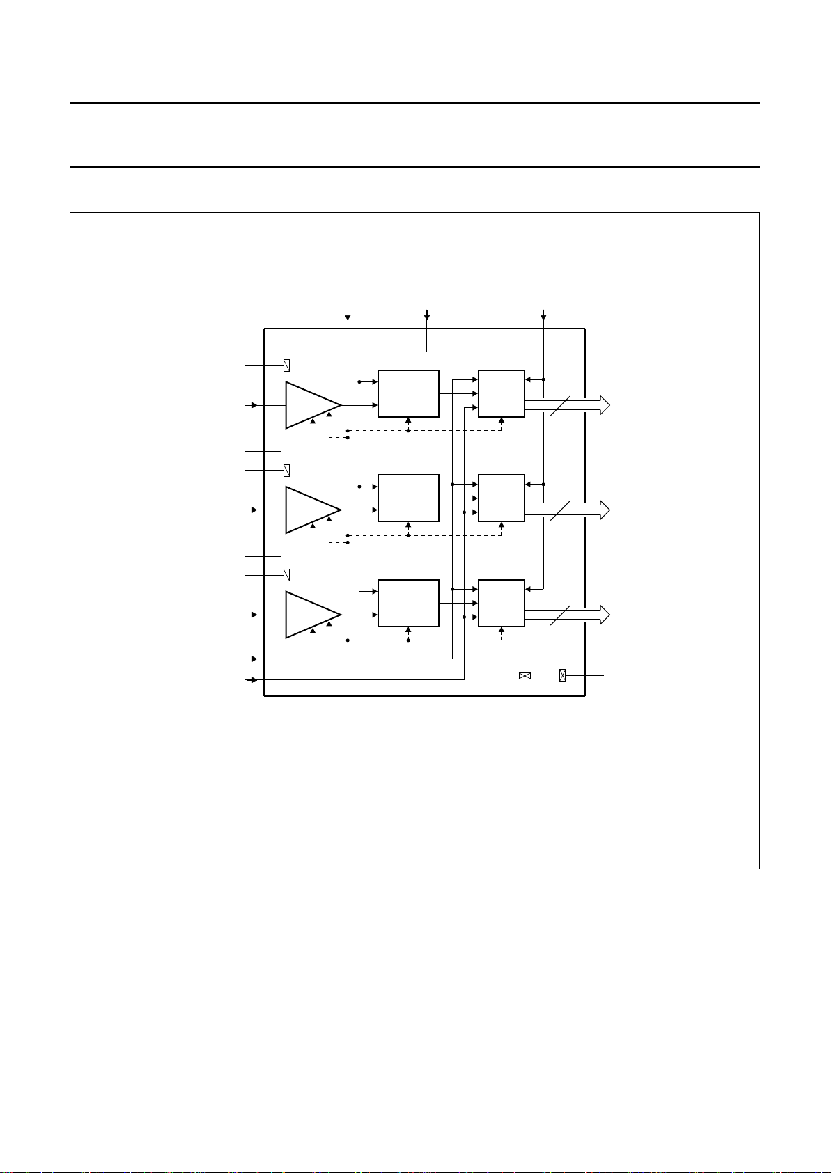
BLOCK DIAGRAM
handbook, full pagewidth
V
V
V
V
DDA1
SSA1
INR
DDA2
SSA2
ING
33
35
34
30
32
31
BUFFER
BUFFER
CLREF CLP CLK
24 23 10
CLAMPING
CIRCUIT
CLAMPING
CIRCUIT
6-BIT
ADC
6-BIT
ADC
38,
40-44
6
3-8
6
TDA8707
R0 to R5
G0 to G5
V
DDA3
V
SSA3
INB
CREFH
CREFL
27
29
28
26
25
BUFFER
36
SLT
TDA8707
CLAMPING
CIRCUIT
Fig.1 Block diagram.
6-BIT
ADC
V
DDD1VSSD1
14-16,
18-20
6
22
21
911
MGA919
B0 to B5
V
DDD2
V
SSD2
1996 Feb 01 3
Philips Semiconductors Product specification
Triple RGB 6-bit video analog-to-digital
interface
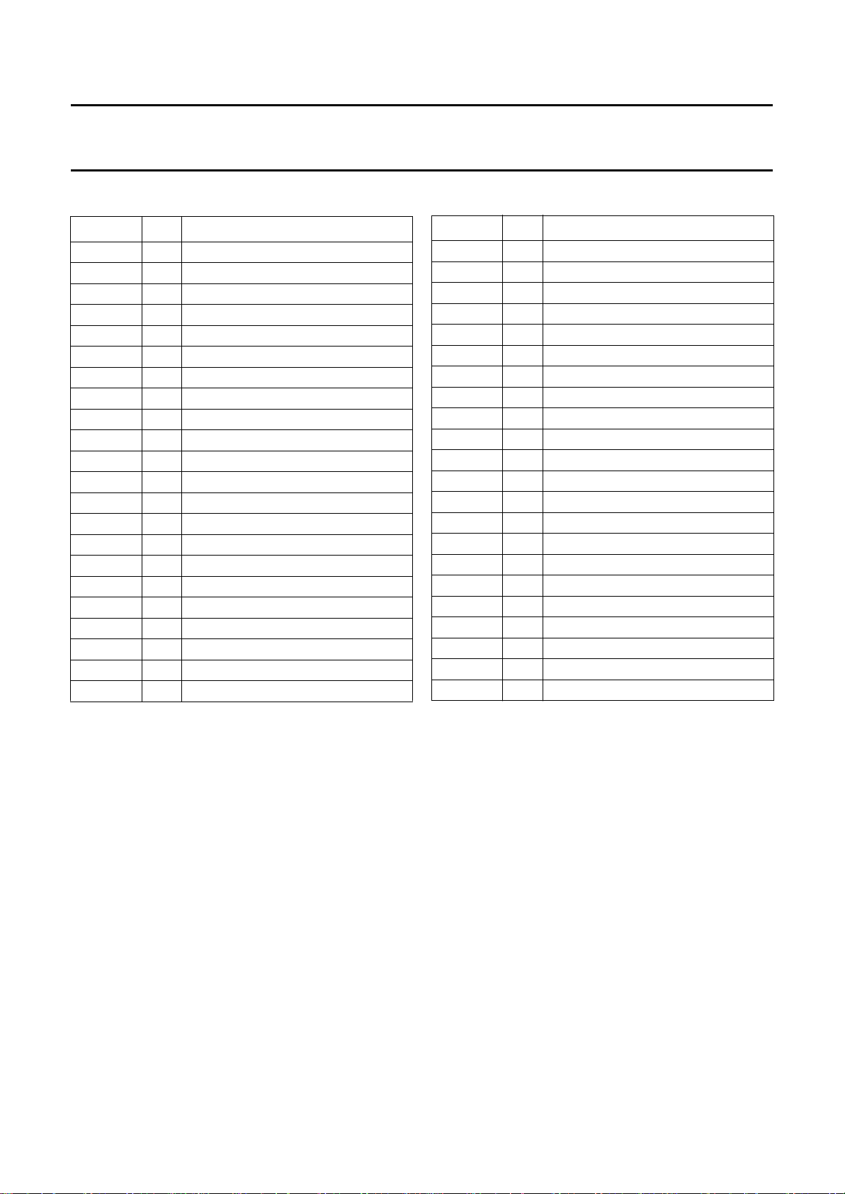
PINNING
SYMBOL PIN DESCRIPTION
n.c. 1 not connected
n.c. 2 not connected
G0 3 GREEN data output; bit 0 (LSB)
G1 4 GREEN data output; bit 1
G2 5 GREEN data output; bit 2
G3 6 GREEN data output; bit 3
G4 7 GREEN data output; bit 4
G5 8 GREEN data output; bit 5 (MSB)
V
SSD1
CLK 10 clock input
V
DDD1
n.c. 12 not connected
n.c. 13 not connected
B0 14 BLUE data output; bit 0 (LSB)
B1 15 BLUE data output; bit 1
B2 16 BLUE data output; bit 2
n.c. 17 not connected
B3 18 BLUE data output; bit 3
B4 19 BLUE data output; bit 4
B5 20 BLUE data output; bit 5 (MSB)
V
SSD2
V
DDD2
9 digital supply ground 1
11 digital supply voltage 1
21 digital supply ground 2
22 digital supply voltage 2
TDA8707
SYMBOL PIN DESCRIPTION
CLP 23 clamping input
CLREF 24 ADCs current reference level input
CREFL 25 converter reference LOW level input
CREFH 26 converter reference HIGH level input
V
DDA3
INB 28 BLUE analog input
V
SSA3
V
DDA2
ING 31 GREEN analog input
V
SSA2
V
DDA1
INR 34 RED analog input
V
SSA1
SLT 36 select input buffer ratio
n.c. 37 not connected
R0 38 RED data output; bit 0 (LSB)
n.c. 39 not connected
R1 40 RED data output; bit 1
R2 41 RED data output; bit 2
R3 42 RED data output; bit 3
R4 43 RED data output; bit 4
R5 44 RED data output; bit 5 (MSB)
27 analog supply voltage 3
29 analog supply ground 3
30 analog supply voltage 2
32 analog supply ground 2
33 analog supply voltage 1
35 analog supply ground 1
1996 Feb 01 4

Philips Semiconductors Product specification
Triple RGB 6-bit video analog-to-digital
interface
R5R4R3R2R1
V
SSD1
V
DDD1
index
corner
n.c.
n.c.
G0
G1
G2
G3
G4
G5
CLK
1
2
3
4
5
6
7
8
9
10
11
44
43
42
41
40
TDA8707
n.c.
39
R0
38
n.c.
37
SLT
36
SSA1
V
35
INR
34
33
32
31
30
29
28
27
26
25
24
23
V
DDA1
V
SSA2
ING
V
DDA2
V
SSA3
INB
V
DDA3
CREFH
CREFL
CLREF
CLP
TDA8707
20
21
B5
SSD2
V
22
DDD2
V
MGA920
12
n.c.
13
n.c.
14
B0
15
B1
16
B2
17
n.c.
B3
18
19
B4
Fig.2 Pin configuration.
LIMITING VALUES
In accordance with the Absolute Maximum Rating System (IEC 134).
SYMBOL PARAMETER CONDITIONS MIN. MAX. UNIT
V
V
∆V
V
V
DDA
DDD
DD
I
i(p-p)
analog supply voltage (pins 27, 30 and 33) −0.3 +6.5 V
digital supply voltage (pins 11 and 22) −0.3 +6.5 V
supply voltage difference between V
input voltage (pins 28, 31 and 34) referenced to V
AC input voltage for switching
DDA
and V
DDD
referenced to V
−0.5 +0.5 V
− V
SSA
− V
SSD
DDA
DDD
V
V
(pins 10 and 23; peak-to-peak value)
T
stg
T
amb
T
j
storage temperature −55 +150 °C
operating ambient temperature −40 +85 °C
junction temperature − +125 °C
THERMAL CHARACTERISTICS
SYMBOL PARAMETER VALUE UNIT
R
th j-a
thermal resistance from junction to ambient in free air 75 K/W
1996 Feb 01 5
 Loading...