

Philips TDA8706, TDA8706T Datasheet
INTEGRATED CIRCUITS
DATA SH EET
TDA8706
6-bit analog-to-digital converter
with multiplexer and clamp
Preliminary specification
Supersedes data of February 1992
File under Integrated Circuits, IC02
1996 Aug 20
Philips Semiconductors Preliminary specification
6-bit analog-to-digital converter with
multiplexer and clamp
FEATURES
• 6-bit resolution
• Binary 3-state TTL outputs
• TTL compatible digital inputs
• 3 multiplexed video inputs
• Luminance and colour difference clamps
• Internal reference
• 300 mW power dissipation
• 20-pin plastic package.
APPLICATIONS
• General purpose video applications
• Y, U and V signals
• Colour Picture-in-Picture (PIPCO) for TV
• Videophone
• Frame grabber.
TDA8706
GENERAL DESCRIPTION
The TDA8706 is a monolithic bipolar 6-bit
Analog-to-Digital Converter (ADC) with a 3 analog input
multiplexer and a clamp. All digital inputs and outputs are
TTL compatible. Regulator with good temperature
compensation.
FUNCTIONAL DESCRIPTION
The TDA8706 is a ‘like-flash’ converter which produces an
output code in one clock period. The device can withstand
a duty clock cycle of 50 to 66.6% (clock HIGH).
Luminance clamping level is fitted with 00H code (output
000000). Chrominance clamping level is fitted with 20H
code (output 100000).
QUICK REFERENCE DATA
Measured over full voltage and temperature ranges.
SYMBOL PARAMETER MIN. TYP. MAX. UNIT
V
V
I
CCA
I
CCD
CCA
CCD
analog supply voltage (pin 2) 4.5 5.0 5.5 V
digital supply voltage (pin 10) 4.5 5.0 5.5 V
analog supply current (pin 20) − 32 39 mA
digital supply current (pin 10) − 28 37 mA
ILE integral linearity error −−±0.75 LSB
DLE DC differential linearity error −−±0.5 LSB
f
CLK
P
T
tot
amb
maximum clock frequency 20 −− MHz
total power dissipation − 300 418 mW
operating ambient temperature range 0 − +70 °C
ORDERING INFORMATION
TYPE
NUMBER
NAME DESCRIPTION VERSION
PACKAGE
TDA8706 DIP20 plastic dual in-line package; 20 leads (300 mil) SOT146-1
TDA8706T SO20 plastic small outline package; 20 leads; body width 7.5 mm SOT163-1
1996 Aug 20 2
Philips Semiconductors Preliminary specification
6-bit analog-to-digital converter with
multiplexer and clamp
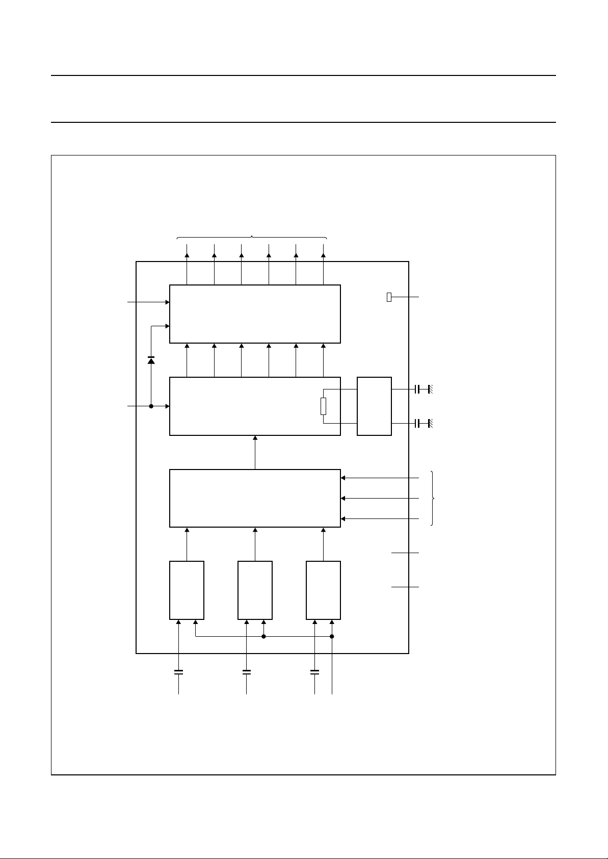
BLOCK DIAGRAM
digital
voltage
17 D3
16 D4
15 D5
chip
enable
TTL
outputs
18 D2
OUTPUTS
19 D1
20 D0
TDA8706
MCD267
ground
input
clock
voltage
reference
CCD
CCA
BOTTOM
TOP
voltage
reference
select
inputs
handbook, full pagewidth
Fig.1 Block diagram.
13 14
ADC
6-BIT
REGULATOR
CBA
11 8 9 10 3 4 1
V
2
V
CLAMP
CHROMINANCE
5
MULTIPLEXER
CLAMP
CHROMINANCE
6
CLAMP
LUMINANCE
12
7
TDA8706
input
chrominance
input
chrominance
1996 Aug 20 3
input
luminance
input
clamp
Philips Semiconductors Preliminary specification
6-bit analog-to-digital converter with
multiplexer and clamp
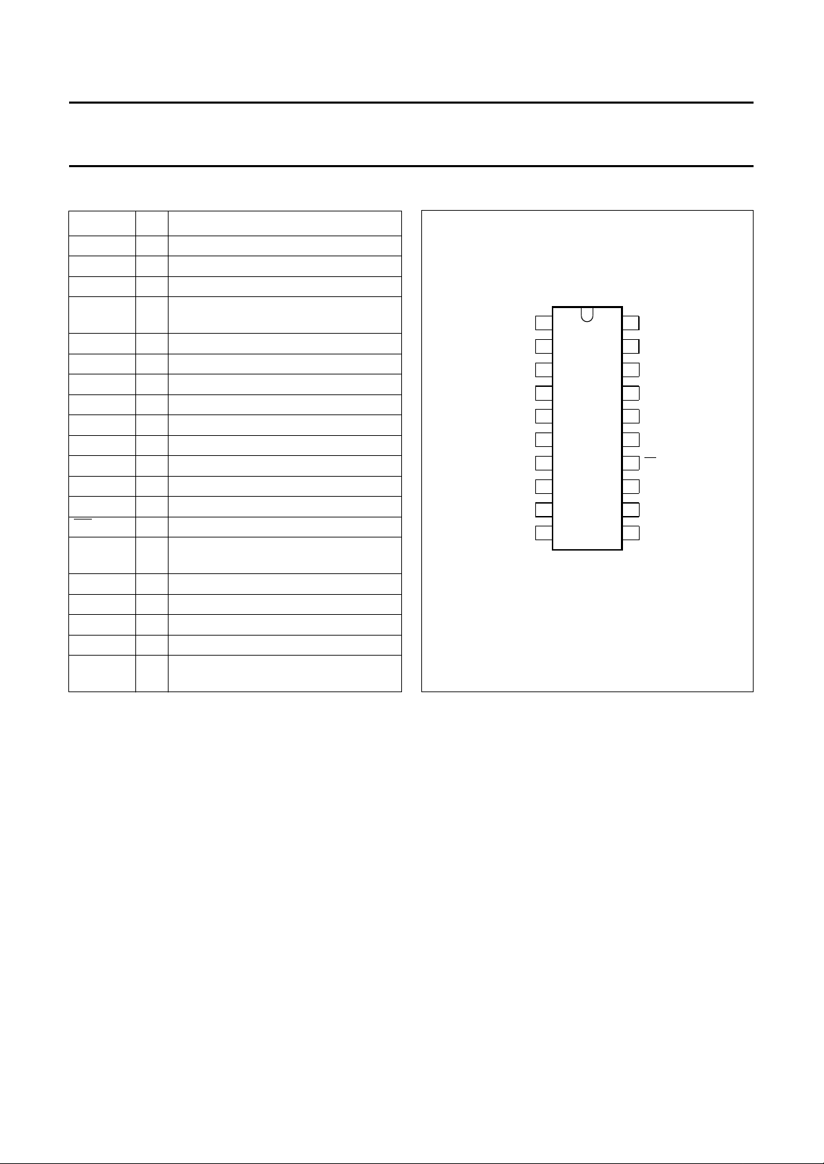
PINNING
SYMBOL PIN DESCRIPTION
GND 1 ground
V
CCA
V
RT
V
RB
INC 5 chrominance input
INB 6 chrominance input
INA 7 luminance input
C 8 select input
B 9 select input
A 10 select input
V
CCD
CLAMP 12 damp pulse input (positive pulse)
CLK 13 clock input
CE 14 chip enable (active LOW)
D5 15 digital voltage output: most significant
D4 16 digital voltage output
D3 17 digital voltage output
D2 18 digital voltage output
D1 19 digital voltage output
D0 20 digital voltage output: significant bit
2 analog positive supply (+5 V)
3 reference voltage TOP decoupling
4 reference voltage BOTTOM
decoupling
11 digital positive supply voltage (+5 V)
bit (MSB)
(LSB)
handbook, halfpage
1
GND
V
2
CCA
V
3
RT
V
4
RB
INC
5
INB
INA
TDA8706
6
7
C
8
B
9
A
10
MCD266
Fig.2 Pin configuration.
TDA8706
D0
20
D1
19
18
D2
D3
17
16
D4
D5
15
14
CE
CLK
13
CLAMP
12
V
11
CCD
1996 Aug 20 4
Philips Semiconductors Preliminary specification
6-bit analog-to-digital converter with
TDA8706
multiplexer and clamp
LIMITING VALUES
In accordance with the Absolute Maximum System (IEC 134).
SYMBOL PARAMETER MIN. MAX. UNIT
V
CCA
V
CCD
− V
V
V
I
T
T
CCA
I
O
stg
amb
CCD
HANDLING
Inputs and outputs are protected against electrostatic discharges in normal handling. However, to be totally safe, it is
desirable to take normal precautions appropriate to handling integrated circuits.
analog supply voltage range (pin 2) −0.3 +7.0 V
digital supply voltage range (pin 10) −0.3 +7.0 V
supply voltage difference 1.0 − V
input voltage range −0.3 +7.0 V
output current − 10 mA
storage temperature range −55 +150 °C
operating ambient temperature range 0 +70 °C
1996 Aug 20 5
 Loading...