

Philips TDA8706AM-C3, TDA8706AM-C1-S1, TDA8706AM-C1 Datasheet
DATA SH EET
Product specification
File under Integrated Circuits, IC02
1996 Jul 30
INTEGRATED CIRCUITS
TDA8706A
6-bit analog-to-digital converter
with multiplexer and clamp
1996 Jul 30 2
Philips Semiconductors Product specification
6-bit analog-to-digital converter
with multiplexer and clamp
TDA8706A
FEATURES
• 6-bit resolution
• Binary 3-state CMOS outputs
• CMOS compatible digital inputs
• 3 multiplexed video inputs
• R, G and B clamps on code 0
• Single 6-bit ADC operation allowed up to 40 MSPS
• External control of clamping level
• Internal reference voltage (external reference allowed)
• Power dissipation only 36 mW (typical)
• Operating temperature of −40 to +85 °C
• Operating between 2.7 and 5.5 V.
APPLICATIONS
• General purpose video applications
• R, G and B signals
• Automotive (car navigation)
• LCD systems
• Frame grabber.
GENERAL DESCRIPTION
The TDA8706A is a 6-bit analog-to-digital converter (ADC)
with 3 analog multiplexed inputs. Each input has an analog
clamp on code 0 for RGB video processing. Clamping
level can also be adjusted externally up to code 20. It can
also be used as a single 6-bit ADC.
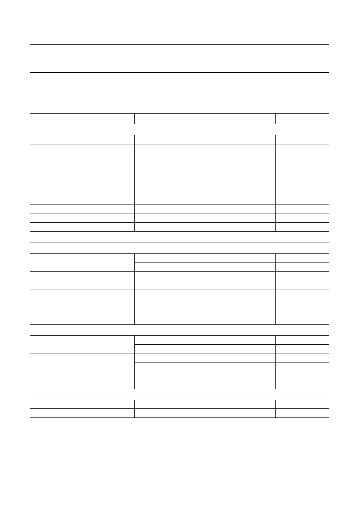
QUICK REFERENCE DATA
ORDERING INFORMATION
SYMBOL PARAMETER CONDITIONS MIN. TYP. MAX. UNIT
V
DDA
analog supply voltage 2.7 3.0 5.5 V
V
DDD
digital supply voltage 2.7 3.0 5.5 V
V
DDO
output stages supply voltage 2.7 3.0 5.5 V
I
DDA
analog supply current − 710mA
I
DDD
digital supply current − 46mA
I
DDO
output stages supply current f
clk
= 40 MHz; ramp input − 1 1.5 mA
INL integral non-linearity f
clk
= 40 MHz; ramp input;
T
amb
=25°C
−±0.25 ±0.6 LSB
DNL differential non-linearity f
clk
= 40 MHz; ramp input;
T
amb
=25°C
−±0.20 ±0.5 LSB
f
clk(max)
maximum clock frequency 40 −−MHz
P
tot
total power dissipation f
clk
= 40 MHz; ramp input
3 V supplies − 36 − mW
5.5 V supplies −−96 mW
TYPE
NUMBER
PACKAGE
NAME DESCRIPTION VERSION
TDA8706AM SSOP24 plastic shrink small outline package; 24 leads; body width 5.3 mm SOT340-1
1996 Jul 30 3
Philips Semiconductors Product specification
6-bit analog-to-digital converter
with multiplexer and clamp
TDA8706A
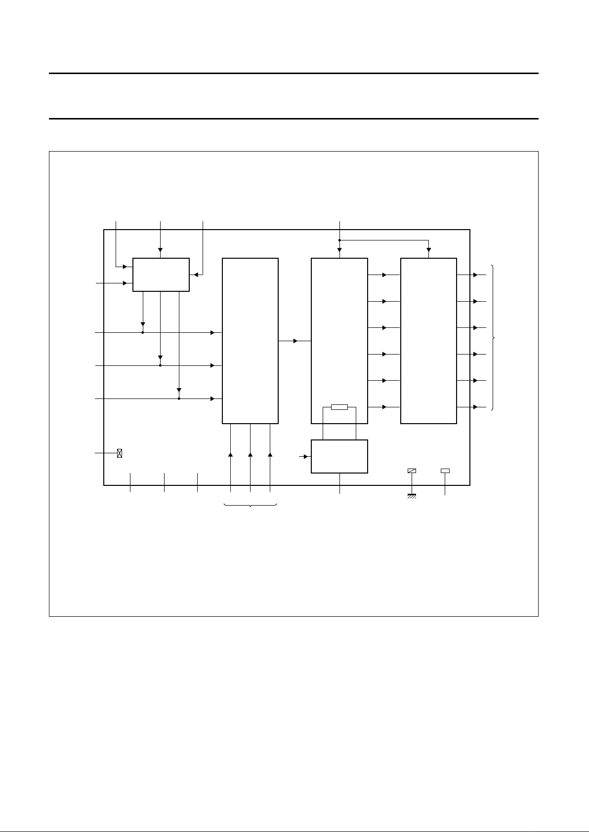
BLOCK DIAGRAM
Fig.1 Block diagram.
handbook, full pagewidth
MULTIPLEXER
6-BIT
ADC
CMOS
OUTPUTS
REGULATOR
4
8
9
10
22
SR SG SB
521
23
123 6 7
14
select
inputs
24
15
131211
D0
16 D1
17 D2
18 D3
19 D4
20 D5
digital
voltage
outputs
MGD133
TDA8706A
CLP
RED
GREEN
BLUE
V
SSD
V
DDOVDDAVDDD
V
DDA
V
RB
V
SSA
V
SSO
CLK
V
CLPB
V
CLPG
V
CLPR
CLAMP
1996 Jul 30 4
Philips Semiconductors Product specification
6-bit analog-to-digital converter
with multiplexer and clamp
TDA8706A
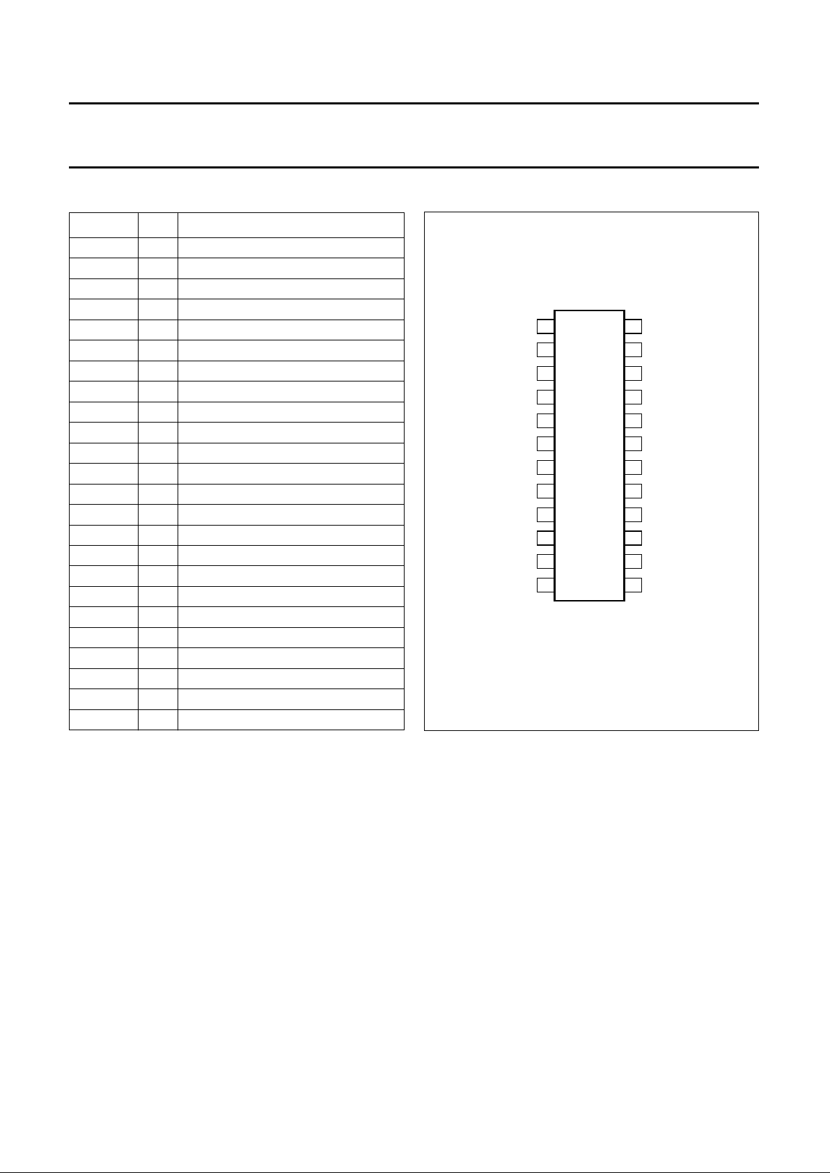
PINNING
SYMBOL PIN DESCRIPTION
SR 1 select input RED
SG 2 select input GREEN
SB 3 select input BLUE
CLP 4 clamping pulse input (positive pulse)
V
DDA
5 analog supply voltage
V
RB
6 reference voltage BOTTOM input
V
SSA
7 analog ground
RED 8 RED input
GREEN 9 GREEN input
BLUE 10 BLUE input
V
CLPR
11 RED clamping voltage level input
V
CLPB
12 BLUE clamping voltage level input
V
CLPG
13 GREEN clamping voltage level input
V
SSO
14 digital output ground
D0 15 digital voltage output; bit 0 (LSB)
D1 16 digital voltage output; bit 1
D2 17 digital voltage output; bit 2
D3 18 digital voltage output; bit 3
D4 19 digital voltage output; bit 4
D5 20 digital voltage output; bit 5
V
DDO
21 supply voltage for output stage
V
SSD
22 digital ground
V
DDD
23 digital supply voltage
CLK 24 clock input
Fig.2 Pin configuration.
handbook, halfpage
TDA8706A
MGD132
1
2
3
4
5
6
7
8
9
10
11
12
24 CLK
V
DDD
V
SSD
V
DDO
D5
D4
D3
D2
D1
D0
V
SSO
V
CLPB
SR
SG
SB
CLP
V
DDA
V
RB
V
SSA
RED
GREEN
BLUE
V
CLPR
V
CLPG
23
22
21
20
19
18
17
16
15
14
13
1996 Jul 30 5
Philips Semiconductors Product specification
6-bit analog-to-digital converter
with multiplexer and clamp
TDA8706A
LIMITING VALUES
In accordance with the Absolute Maximum Rating System (IEC 134).
HANDLING
Inputs and outputs are protected against electrostatic discharges in normal handling. However, to be totally safe, it is
desirable to take normal precautions appropriate to handling integrated circuits.
THERMAL CHARACTERISTICS
SYMBOL PARAMETER MIN. MAX. UNIT
V
DDA
analog supply voltage −0.3 +7.0 V
V
DDD
digital supply voltage −0.3 +7.0 V
∆V
DD
supply voltage difference
V
DDA
− V
DDD
−1.0 +1.0 V
V
DDA
− V
DDO
−1.0 +1.0 V
V
DDD
− V
DDO
−1.0 +1.0 V
V
I
input voltage −0.3 +7.0 V
I
O
output current − 10 mA
T
stg
storage temperature −55 +150 °C
T
amb
operating ambient temperature −40 +85 °C
T
j
junction temperature − +150 °C
SYMBOL PARAMETER VALUE UNIT
R
th j-a
thermal resistance from junction to ambient in free air 119 K/W
1996 Jul 30 6
Philips Semiconductors Product specification
6-bit analog-to-digital converter
with multiplexer and clamp
TDA8706A
CHARACTERISTICS
V
DDA=V5
to V7= 2.7 to 5.5 V; V
DDD=V23
to V22= 2.7 to 5.5 V; V
DDO=V21
to V14= 2.7 to 5.5 V;
V
SSA,VSSD
and V
SSO
shorted together; V
i(p-p)
= 0.7 V; T
amb
= −40 to +85 °C; typical values measured at
V
DDA=VDDD=VDDO
= 3 V and T
amb
=25°C; unless otherwise specified.
SYMBOL PARAMETER CONDITIONS MIN. TYP. MAX. UNIT
Supply
V
DDA
analog supply voltage 2.7 3.0 5.5 V
V
DDD
digital supply voltage 2.7 3.0 5.5 V
V
DDO
output stages supply
voltage
2.7 3.0 5.5 V
∆V
DD
supply voltage difference
V
DDA
− V
DDD
−0.3 − +0.3 V
V
DDA
− V
DDO
−0.3 − +0.3 V
V
DDD
− V
DDO
−0.3 − +0.3 V
I
DDA
analog supply current − 710mA
I
DDD
digital supply current − 46mA
I
DDO
output stages supply current f
clk
= 40 MHz; ramp input − 1 1.5 mA
Inputs
C
LOCK INPUT CLK (REFERENCED TO V
SSD
); note 1
V
IL
LOW level input voltage 0 − V
DDD
× 0.3 V
V
DDD
< 3.3 V 0 − V
DDD
× 0.2 V
V
IH
HIGH level input voltage V
DDD
× 0.7 − V
DDD
V
V
DDD
< 3.3 V V
DDD
× 0.8 − V
DDD
V
I
IL
LOW level input current V
clk=VDDD
× 0.2 −10 +1µA
I
IH
HIGH level input current V
clk=VDDD
× 0.8 − 210µA
Z
i
input impedance f
clk
= 40 MHz − 4 − kΩ
C
I
input capacitance f
clk
= 40 MHz − 3 − pF
INPUTS SR, SG, SB, CLP (REFERENCED TO V
SSD
)
V
IL
LOW level input voltage 0 − V
DDD
× 0.3 V
V
DDD
< 3.3 V 0 − V
DDD
× 0.2 V
V
IH
HIGH level input voltage V
DDD
× 0.7 − V
DDD
V
V
DDD
< 3.3 V V
DDD
× 0.8 − V
DDD
V
I
IL
LOW level input current VIL=V
DDD
× 0.2 −1 −−µA
I
IH
HIGH level input current VIH=V
DDD
× 0.8 −− +1 µA
INPUTS V
CLPR,VCLPG
AND V
CLPB
(REFERENCED TO V
SSA
); see Tables 1 and 2
V
CLP
input voltage for clamping V
code −9
− V
code 20
V
I
CLP
input current −− 30 µA
 Loading...