

Philips TDA8702T, TDA8702 Datasheet
INTEGRATED CIRCUITS
DATA SH EET
TDA8702
8-bit video digital-to-analog
converter
Product specification
Supersedes data of April 1993
File under Integrated Circuits, IC02
1996 Aug 23
Philips Semiconductors Product specification
8-bit video digital-to-analog converter TDA8702
FEATURES
• 8-bit resolution
• Conversion rate up to 30 MHz
• TTL input levels
• Internal reference voltage generator
• Two complementary analog voltage outputs
• No deglitching circuit required
• Internal input register
APPLICATIONS
• High-speed digital-to-analog conversion
• Digital TV including:
– field progressive scan
– line progressive scan
• Subscriber TV decoders
• Satellite TV decoders
• Digital VCRs.
• Low power dissipation
• Internal 75 Ω output load (connected to the analog
supply)
• Very few external components required.
GENERAL DESCRIPTION
The TDA8702 is an 8-bit Digital-to-Analog Converter
(DAC) for video and other applications. It converts the
digital input signal into an analog voltage output at a
maximum conversion rate of 30 MHz. No external
reference voltage is required and all digital inputs are TTL
compatible.
QUICK REFERENCE DATA
SYMBOL PARAMETER CONDITIONS MIN. TYP. MAX. UNIT
V
V
I
CCA
I
CCD
V
CCA
CCD
OUT
− V
analog supply voltage 4.5 5.0 5.5 V
digital supply voltage 4.5 5.0 5.5 V
analog supply current note 1 − 26 32 mA
digital supply current note 1 − 23 30 mA
full-scale analog output voltage
OUT
(peak-to-peak value)
note 2
=10kΩ−1.45 −1.60 −1.75 V
Z
L
=75kΩ−0.72 −0.80 −0.88 V
Z
L
ILE DC integral linearity error −−±1/2 LSB
DLE DC differential linearity error −−±1/2 LSB
f
CLK
B −3 dB analog bandwidth f
P
tot
maximum conversion rate −−30 MHz
= 30 MHz; note 3 − 150 − MHz
CLK
total power dissipation − 250 340 mW
Note
1. D0 to D7 connected to V
2. The analog output voltages (V
between V
and each of these outputs is typically 75 Ω.
CCA
and CLK connected to DGND.
CCD
OUT
and V
) are negative with respect to V
OUT
(see Table 1). The output resistance
CCA
3. The −3 dB analog output bandwidth is determined by real time analysis of the output transient at a maximum input
code transition (code 0 to 255).
1996 Aug 23 2

Philips Semiconductors Product specification
8-bit video digital-to-analog converter TDA8702
ORDERING INFORMATION
TYPE
NUMBER
NAME DESCRIPTION VERSION
PACKAGE
TDA8702 DIP16 plastic dual in-line package; 16 leads (300 mil); long body SOT38-1
TDA8702T SO16 plastic small outline package; 16 leads; body width 7.5 mm SOT162-1
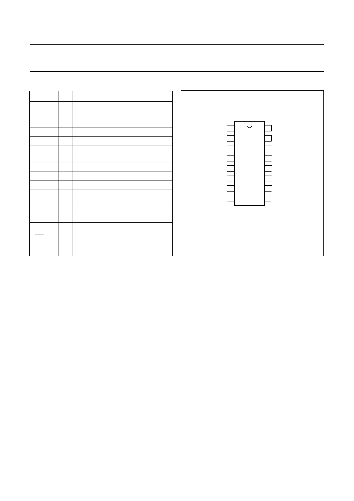
BLOCK DIAGRAM
CLK
1
REFERENCE
6
2
5
CLOCK INPUT
INTERFACE
BAND-GAP
CURRENT
REFERENCE
LOOP
CURRENT
GENERATORS
CURRENT
SWITCHES
16
V
CCA
75
75
Ω
Ω
15
V
V
OUT
OUT
14
handbook, full pagewidth
REF
100 nF
DGND
AGND
TDA8702/
TDA8702T
D1
D2
D3
D4
D5
D6
12
11
3
4
10
9
8
7
(LSB) D0
(MSB) D7
Fig.1 Block diagram.
1996 Aug 23 3
REGISTERS
DATA
INPUT
INTERFACE
13
MSA659
V
CCD
Philips Semiconductors Product specification
8-bit video digital-to-analog converter TDA8702
PINNING
SYMBOL PIN DESCRIPTION
REF 1 voltage reference (decoupling)
AGND 2 analog ground
D2 3 data input; bit 2
D3 4 data input; bit 3
CLK 5 clock input
DGND 6 digital ground
D7 7 data input; bit 7
D6 8 data input; bit 6
D5 9 data input; bit 5
D4 10 data input; bit 4
D1 11 data input; bit 1
D0 12 data input; bit 0
V
CCD
13 positive supply voltage for digital
circuits (+5 V)
V
V
V
OUT
OUT
CCA
14 analog voltage output
15 complementary analog voltage output
16 positive supply voltage for analog
circuits (+5 V)
handbook, halfpage
1
REF
2
AGND
D2
3
4
D3
CLK
DGND
D7
D6
TDA8702/
TDA8702T
5
6
7
8
MSA658
Fig.2 Pin configuration.
V
16
CCA
V
15
OUT
V
14
OUT
V
13
CCD
D0
12
D1
11
D4
10
D5
9
1996 Aug 23 4

Philips Semiconductors Product specification
8-bit video digital-to-analog converter TDA8702
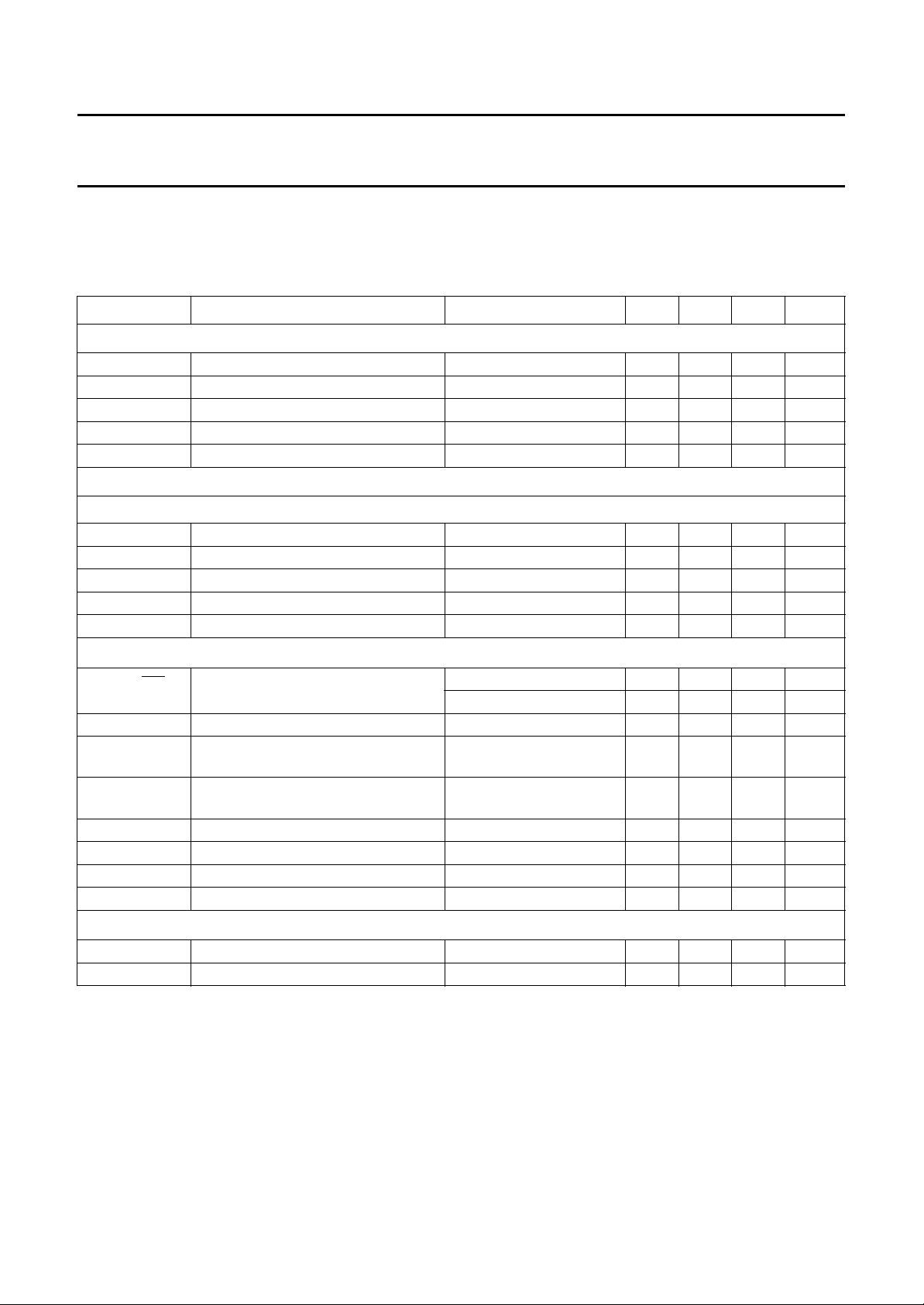
LIMITING VALUES
In accordance with the Absolute Maximum Rating System (IEC 134).
SYMBOL PARAMETER MIN. MAX. UNIT
V
CCA
V
CCD
− V
V
CCA
CCD
AGND − DGND ground voltage differential −0.1 +0.1 V
V
I
I
OUT/IOUT
T
stg
T
amb
T
j
HANDLING
analog supply voltage −0.3 +7.0 V
digital supply voltage −0.3 +7.0 V
supply voltage differential −0.5 +0.5 V
input voltage (pins 3 to 5 and 7 to 12) −0.3 V
CCD
V
total output current (pins 14 and 15) −5 +26 mA
storage temperature −55 +150 °C
operating ambient temperature 0 +70 °C
junction temperature − +125 °C
Inputs and outputs are protected against electrostatic discharges in normal handling. However, to be totally safe, it is
desirable to take normal precautions appropriate to handling integrated circuits.
THERMAL RESISTANCE
SYMBOL PARAMETER VALUE UNIT
R
th j-a
from junction to ambient in free air
SOT38-1 70 K/W
SOT162-1 90 K/W
1996 Aug 23 5
Philips Semiconductors Product specification
8-bit video digital-to-analog converter TDA8702
CHARACTERISTICS
V
CCA=V16
AGND by a 100 nF capacitor; T
(typical values measured at V
SYMBOL PARAMETER CONDITIONS MIN. TYP. MAX. UNIT
Supply
V
CCA
V
CCD
I
CCA
I
CCD
AGND − DGND ground voltage differential −0.1 − +0.1 V
Inputs
IGITAL INPUTS (D7 TO D0) AND CLOCK INPUT (CLK)
D
V
IL
V
IH
I
IL
I
IH
f
CLK
Outputs (note 2; referenced to V
V
OUT
V
OS
V
OUT
V
OS
B −3 dB analog bandwidth note 3; f
G
diff
Φ
diff
Z
O
Transfer function (f
ILE DC integral linearity error −−±1/2 LSB
DLE DC differential linearity error −−±1/2 LSB
− V2= 4.5 V to 5.5 V; V
amb
CCA=VCCD
CCD=V13
=0°C to +70 °C; AGND and DGND shorted together; unless otherwise specified
− V6= 4.5 V to 5.5 V; V
= 5 V and T
analog supply voltage 4.5 5.0 5.5 V
digital supply voltage 4.5 5.0 5.5 V
analog supply current note 1 − 26 32 mA
digital supply current note 1 − 23 30 mA
LOW level input voltage 0 − 0.8 V
HIGH level input voltage 2.0 − V
LOW level input current VI= 0.4 V −−0.3 −0.4 mA
HIGH level input current VI= 2.7 V − 0.01 20 µA
maximum clock frequency −−30 MHz
)
CCA
− V
OUT
full-scale analog output voltages
(peak-to-peak value)
analog offset output voltage code = 0 −−3−25 mV
/TC full-scale analog output voltage
temperature coefficient
/TC analog offset output voltage
temperature coefficient
differential gain − 0.6 − %
differential phase − 1 − deg
output impedance − 75 −Ω
= 30 MHz)
CLK
amb
=25°C).
CCA
− V
= −0.5 V to +0.5 V; V
CCD
REF
ZL=10kΩ−1.45 −1.60 −1.75 V
=75Ω−0.72 −0.80 −0.88 V
Z
L
−−200 µV/K
−−20 µV/K
= 30 MHz − 150 − MHz
CLK
decoupled to
V
CCD
1996 Aug 23 6
 Loading...