

Philips TDA8601 Datasheet

INTEGRATED CIRCUITS
DATA SH EET
TDA8601
RGB/YUV and fast blanking switch
Product specification
Supersedes data of July 1994
File under Integrated Circuits, IC02
1996 Jun 27

Philips Semiconductors Product specification
RGB/YUV and fast blanking switch TDA8601
FEATURES
• YUV/RGB and fast blanking switch
• 3-state output
• Selectable clamp:
– passive (with diodes) or
– active clamp
• Bandwidth greater than 22 MHz
• Fully ESD protected
• Latch-up free.
GENERAL DESCRIPTION
The device is intended for switching between two RGB or
YUV video sources. The outputs can be set to a
high-impedance state to enable parallel connection of
several devices.
A HIGH level on SEL (pin 5) selects the video inputs of
Channel 2. The IOCNTR control pin (pin 16) defines the
3-state outputs and clamp inputs:
• HIGH = 3-state outputs (also for test; active clamp)
• LOW = passive clamp at the video inputs (diode)
• Sandcastle: the video signal is clamped with an active
APPLICATIONS
clamp during the sync pulse.
• Standard and high definition television sets
• Peri-television sets.
QUICK REFERENCE DATA
SYMBOL PARAMETER CONDITIONS MIN. TYP. MAX. UNIT
V
P
G
v
supply voltage 7.2 8.0 8.8 V
voltage gain −0.5 0 +0.5 dB
B bandwidth at 3 dB 22 −−MHz
α
ct
crosstalk attenuation between two
fi= 5 MHz −60 −−dB
video channels
T
amb
operating ambient temperature 0 − 70 °C
ORDERING INFORMATION
TYPE
NUMBER
NAME DESCRIPTION VERSION
PACKAGE
TDA8601 DIP16 plastic dual in-line package; 16 leads (300 mil); long body SOT38-1
TDA8601T SO16 plastic small outline package; 16 leads; body width 3.9 mm SOT109-1
1996 Jun 27 2

Philips Semiconductors Product specification
RGB/YUV and fast blanking switch TDA8601
BLOCK DIAGRAM
Fig.1 Block diagram.
1996 Jun 27 3
Philips Semiconductors Product specification
RGB/YUV and fast blanking switch TDA8601
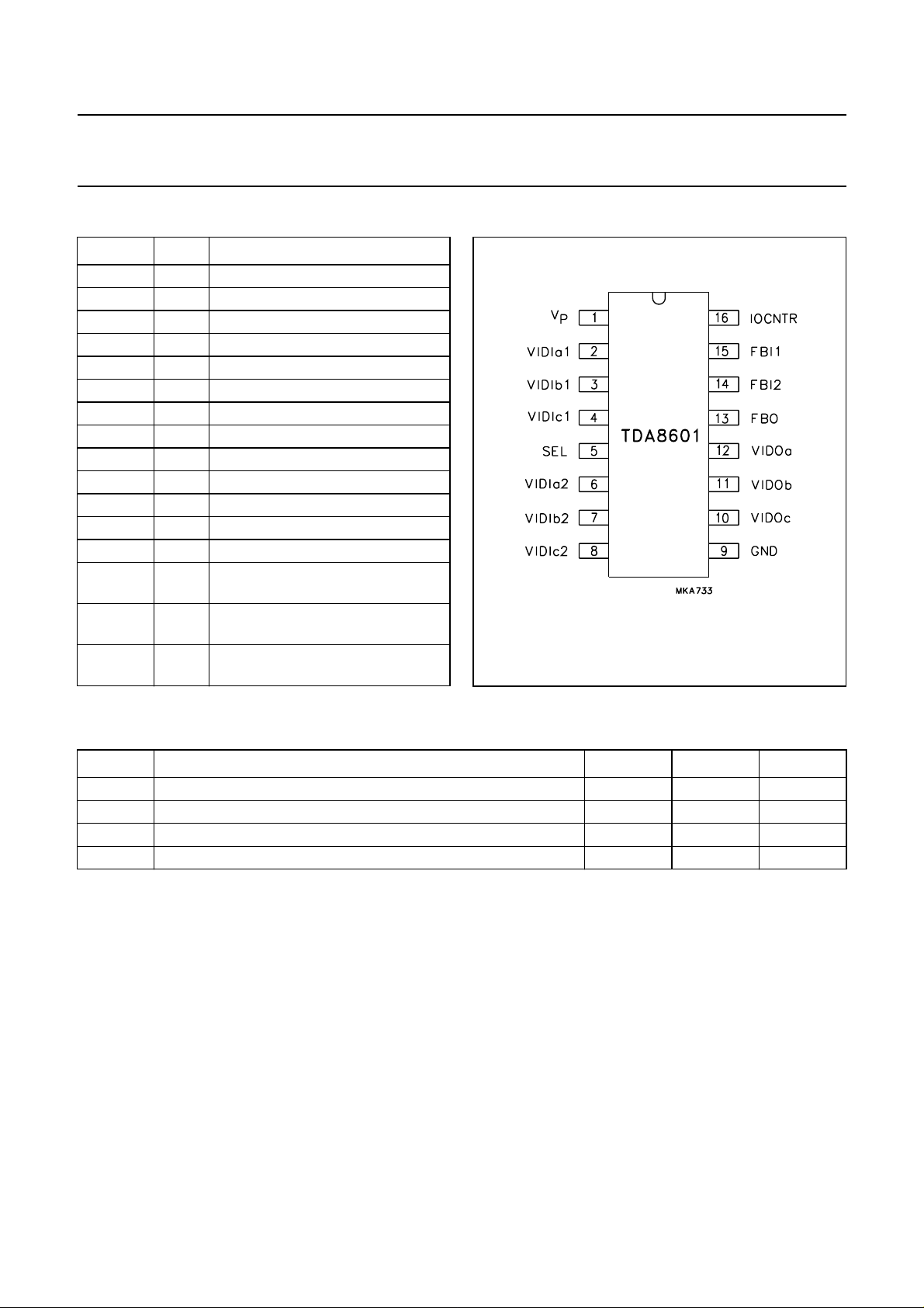
PINNING
SYMBOL PIN DESCRIPTION
V
P
VIDIa1 2 video input a (channel 1)
VIDIb1 3 video input b (channel 1)
VIDIc1 4 video input c (channel 1)
SEL 5 channel selection
VIDIa2 6 video input a (channel 2)
VIDIb2 7 video input b (channel 2)
VIDIc2 8 video input c (channel 2)
GND 9 ground
VIDOc 10 video output c
VIDOb 11 video output b
VIDOa 12 video output a
FBO 13 fast blanking output signal
FBI2 14 fast blanking input signal
FBI1 15 fast blanking input signal
IOCNTR 16 control of video input or video
1 supply voltage (8 V)
(channel 2)
(channel 1)
Fig.2 Pin configuration.
output
LIMITING VALUES
In accordance with the Absolute Maximum Rating System (IEC 134).
SYMBOL PARAMETER MIN. MAX. UNIT
V
P
V
i
T
j
T
stg
supply voltage −0.3 +12 V
input voltage (pins 2 to 4 and 6 to 8) referenced to ground 0 8.8 V
junction temperature − 150 °C
IC storage temperature −55 +150 °C
HANDLING
Inputs and outputs are protected against electrostatic discharge in normal handling. However, to be totally safe, it is
desirable to take normal precautions appropriate to handling MOS devices.
ESD in accordance with
“MIL STD 883C” -“Method 3015”
:
1. Human body model: 1500 Ω, 100 pF, 3 pulses positive and 3 pulses negative on each pin with respect to ground.
Class 2: 2000 to 3999 V.
2. Machine model: 0 Ω, 200 pF, 3 pulses positive and 3 pulses negative on each pin with respect to ground. The IC
withstands 200 V.
1996 Jun 27 4
Philips Semiconductors Product specification
RGB/YUV and fast blanking switch TDA8601
THERMAL CHARACTERISTICS
SYMBOL PARAMETER VALUE UNIT
R
th j-a
OPERATING CHARACTERISTICS
The operating characteristics are the conditions within the IC when it is functional; these conditions can have any value.
For example, condition V
voltage range.
SYMBOL PARAMETER CONDITIONS MIN. TYP. MAX. UNIT
Supply
V
P
Video inputs (pins 1 to 3 and 6 to 8)
V
i(p-p)
C
i
Control inputs (pins 5 and 16)
V
IH
V
IL
V
IH
V
IL
V
sc
t
W
thermal resistance from junction to ambient in free air
DIP16 70 K/W
SO16 115 K/W
(pin 5) is fixed at 0.5 V. The IC will then operate over the full temperature range and supply
IL
supply voltage 7.2 8.0 8.8 V
input video signal amplitude
(peak-to-peak value)
R, G, B signals − 0.7 1 V
Y signal; active clamp − 1 1.4 V
−(B − Y) signal; active clamp − 1.05 1.5 V
−(R − Y) signal; active clamp − 1.33 1.9 V
input clamp capacitor − 47 − nF
HIGH level input voltage (pin 5) IIH=10µA 0.9 − V
P
V
LOW level input voltage (pin 5) IIL= −10 µA −−0.5 V
HIGH level input voltage (pin 16) IIH=10µA 2.0 − V
P
V
LOW level input voltage (pin 16) IIL= −10 µA −−0.8 V
sandcastle input voltage level
(pin 16)
zero level −−1.1 V
blanking level 2.0 − 3.1 V
clamp level 3.9 − 5.5 V
clamp pulse width SECAM mode − 3.6 −µs
PAL mode − 2.5 −µs
Fast blanking inputs (pins 14 and 15)
V
IH
V
IL
HIGH level input voltage 0.95 − V
LOW level input voltage −−0.5 V
Video outputs (pins 10 to 12)
C
L
R
L
output load capacitor − 40 100 pF
output load resistor note 1 1 −−kΩ
1996 Jun 27 5
P
V

Philips Semiconductors Product specification
RGB/YUV and fast blanking switch TDA8601
SYMBOL P ARAMETER CONDITIONS MIN. TYP . MAX. UNIT
Fast blanking output (pin 13)
C
L
R
L
Note
1. For the DIP16 package, the thermal resistance is lower. The minimum value for the output load resistor is 270 Ω.
CHARACTERISTICS
The typical values are given for V
Fig.8 over full supply voltage and temperature range; unless otherwise specified.
SYMBOL PARAMETER CONDITIONS MIN. TYP. MAX. UNIT
Supply
I
P
SVRR supply voltage rejection ratio f
Video inputs (pins 1 to 3 and 4 to 6)
R
i
C
i(max)
V
clamp
I
sink
I
clamp
output load capacitor − 40 100 pF
output load resistor note 1 1 −−kΩ
=8V; T
P
supply current no resistive load on the
=25°C. CL= 40 pF; no load resistor; measured in application circuit of
amb
− 33 40 mA
outputs
= 40 Hz to 50 kHz; note 1 −−−36 dB
i
f
= 40 Hz; note 1 −−51 −36 dB
i
input resistance for each type of clamp 10 −−kΩ
maximum input capacitance − 3 − pF
input clamping voltage level Ii= −50 mA; passive clamp 1.05 1.21 1.35 V
I
= 50 mA; active clamp;
i
V
I
i
V
= 3.9 V
IOCNTR
= −50 mA; active clamp;
= 3.9 V
IOCNTR
2.05 2.42 2.70 V
2.05 2.37 2.70 V
input sink current Vi= 2 V; passive clamp 0.5 1.6 3 µA
maximum absolute input clamping
current
Vi=V
clamp
active clamp
+ 0.5 V;
200 −−µA
1996 Jun 27 6
 Loading...