

Philips TDA8586Q-N1-S421 Datasheet

DATA SH EET
Preliminary specification
Supersedes data of 1998 May 25
File under Integrated Circuits, IC01
1999 Apr 08
INTEGRATED CIRCUITS
TDA8586
Power amplifier with load detection
and auto BTL/SE selection

1999 Apr 08 2
Philips Semiconductors Preliminary specification
Power amplifier with load detection and
auto BTL/SE selection
TDA8586
FEATURES
General
• Operating voltage from 8 to 18 V
• Low distortion
• Few external components, fixed gain
• Automatic mode selection (SE or BTL) depending on
connected ‘rear’ loads
• Can be used as a stereo amplifier in Bridge-Tied Load
(BTL) or quad Single-Ended (SE) amplifiers
• Single-ended mode without loudspeaker capacitor
• Soft clipping, to guarantee good clip behaviour with
inductive loads
• Mute and standby mode with one-pin operation
• Diagnostic information for Dynamic Distortion Detector
(DDD), high temperature (140 °C) mode of operation
and short-circuit
• No switch-on/off plops when switching between standby
and mute and from mute to on
• Load detection on ‘rear’ channels when switching from
standby to mute
• Fast mute on supply voltage drops (low V
P
mute).
Protection
• Short-circuit proof to ground, positive supply voltage on
all pins and across load
• ESD protected on all pins
• Thermal protection against temperatures exceeding
150 °C
• Load dump protection
• Overvoltage protection.
GENERAL DESCRIPTION
The IC incorporates the following functions:
1. 4 × 6 W SE amplifies without SE capacitor, because of
the availability of 2 half supply voltage power buffers
2. 2 × 20 W BTL amplifiers
3. Automatic switching between 2 and 4 speaker
operation. The mode of operation is determined during
start-up.
This amplifier is protected for all general short-circuit
conditions to battery or ground, overvoltage, 45 V load
dump and short-circuits on the speaker outputs.
The IC is contained in a 20-pin power HSOP package, but
is also available in a 17-pin SIL power package. When
packaged in the 20-pin HSOP package additional
functions are available:
1. DDD level selection between 2 and 10%
2. Overrule pin for changing mode of operation
(from SE to BTL or from BTL to SE).
ORDERING INFORMATION
TYPE
NUMBER
PACKAGE
NAME DESCRIPTION VERSION
TDA8586Q DBS17P plastic DIL-bent-SIL power package; 17 leads (lead length 12 mm) SOT243-1
TDA8586TH HSOP20 heatsink small outline package; 20 leads; low stand-off SOT418-2

1999 Apr 08 3
Philips Semiconductors Preliminary specification
Power amplifier with load detection and
auto BTL/SE selection
TDA8586
QUICK REFERENCE DATA
SYMBOL PARAMETER CONDITIONS MIN. TYP. MAX. UNIT
V
P
operating supply voltage 8.0 − 18 V
I
q(tot)
total quiescent current VP= 14.4 V, SE mode − 140 170 mA
I
stb
standby supply current VP= 14.4 V − 1 100 µA
G
v
voltage gain SE mode 25 26 27 dB
BTL mode 31 32 33 dB
Bridge-tied load application
P
o
output power VP= 14.4 V; RL=4Ω
THD = 0.5% 14 15 − W
THD = 10% 17 21 − W
THD total harmonic distortion f
i
= 1 kHz; Po=1W;
VP= 14.4 V; RL=4Ω
− 0.05 0.15 %
V
OO
DC output offset voltage VP= 14.4 V; RL=4Ω;
mute condition
− 10 20 mV
V
P
= 14.4 V; on condition − 0 100 mV
V
n(o)
noise output voltage Rs=1kΩ; VP= 14.4 V − 100 200 µV
Single-ended application
P
o
output power VP= 14.4 V; RL=4Ω
THD = 0.5% 4 4.5 − W
THD = 10% 5 6 − W
THD total harmonic distortion f
i
= 1 kHz; Po=1W;
VP= 14.4 V; RL=4Ω
− 0.08 0.15 %
V
OO
DC output offset voltage VP= 14.4 V; RL=4Ω;
mute condition
− 10 20 mV
V
P
= 14.4 V; on condition − 0 100 mV
V
n(o)
noise output voltage Rs=1kΩ; VP= 14.4 V − 80 150 µV

1999 Apr 08 4
Philips Semiconductors Preliminary specification
Power amplifier with load detection and
auto BTL/SE selection
TDA8586
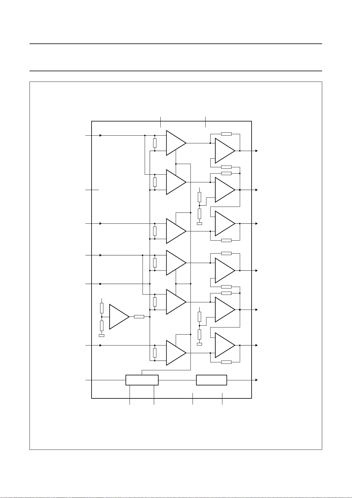
BLOCK DIAGRAM
Fig.1 Block diagram SOT243-1.
handbook, full pagewidth
MGR023
1
OUT1
ACREF
11
IN3
7
IN2
6
IN1
5
IN4
8
MSO
13
V/I
+
−
OA
+
−
4
OUT2
OA
+
−
OA
+
−
3
HVP1
V
Pn
V
Pn
60
kΩ
V/I
+
−
60
kΩ
V/I
+
−
60
kΩ
17
OUT3
V/I
+
−
OA
+
−
14
OUT4
12
DIAG
OA
+
−
OA
+
−
15
HVP2
60
kΩ
V/I
+
−
60
kΩ
BUFFER
V
Pn
30 kΩ
V/I
+
−
60
kΩ
INTERFACE DIAGNOSTIC
10
PGND2
V
P1
2
V
P2
16
9
PGND1
TDA8586Q
1999 Apr 08 5
Philips Semiconductors Preliminary specification
Power amplifier with load detection and
auto BTL/SE selection
TDA8586
Fig.2 Block diagram SOT418-2 (HSOP20 heatsink up).
handbook, full pagewidth
MGR024
17
OUT1
ACREF
6
IN3
4
IN2
3
IN1
2
IN4
5
MSO
8
n.c.
1
V/I
+
−
OA
+
−
20
OUT2
OA
+
−
OA
+
−
19
HVP1
V
Pn
V
Pn
60
kΩ
V/I
+
−
60
kΩ
V/I
+
−
60
kΩ
14
OUT3
V/I
+
−
OA
+
−
11
OUT4
7
DIAG
OA
+
−
OA
+
−
12
HVP2
60
kΩ
V/I
+
−
60
kΩ
BUFFER
V
Pn
30 kΩ
V/I
+
−
60
kΩ
INTERFACE DIAGNOSTIC
10
DDDSEL9OVERRULE
15
PGND2
V
P1
18
V
P2
13
16
PGND1
TDA8586TH

1999 Apr 08 6
Philips Semiconductors Preliminary specification
Power amplifier with load detection and
auto BTL/SE selection
TDA8586
PINNING
SYMBOL
PIN
SOT243
PIN
SOT418
DESCRIPTION
n.c. − 1 not connected
IN1 5 2 non-inverting input 1
IN2 6 3 inverting input 2
IN3 7 4 non inverting input 3
IN4 8 5 inverting input 4
ACREF 11 6 common signal input
DIAG 12 7 diagnostic output/mode fix
MSO 13 8 mode select mute, standby or on
OVERRULE − 9 mode selection overrule
DDDSEL − 10 2 or 10% dynamic distortion detection
OUT4 14 11 SE output 4 (negative)
HVP2 15 12 buffer output/BTL output 2 (negative)
V
P2
16 13 supply voltage 2
OUT3 17 14 SE output 3/BTL output 2 (positive)
PGND2 10 15 power ground 2
PGND1 9 16 power ground 1
OUT1 1 17 SE output 1/BTL output 1 (positive)
V
P1
2 18 supply voltage 1
HVP1 3 19 buffer output/BTL output 1 (negative)
OUT2 4 20 SE output 2 (negative)
1999 Apr 08 7
Philips Semiconductors Preliminary specification
Power amplifier with load detection and
auto BTL/SE selection
TDA8586
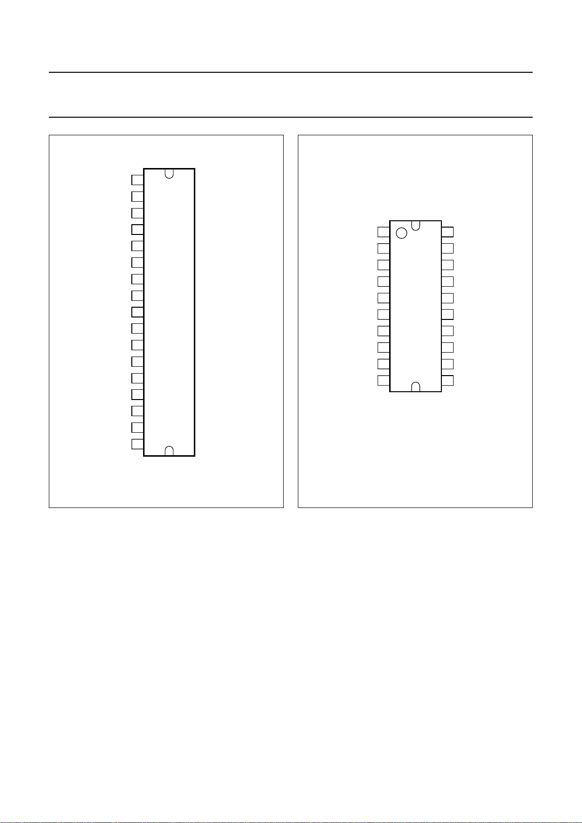
Fig.3 Pin configuration (SOT243-1).
handbook, halfpage
TDA8586Q
MGR025
OUT1
V
P1
HVP1
OUT2
IN1
IN2
IN3
IN4
PGND1
PGND2
ACREF
DIAG
MSO
OUT4
HVP2
V
P2
OUT3
1
2
3
4
5
6
7
8
9
10
11
12
13
14
15
16
17
Fig.4 Pin configuration (SOT418-2).
handbook, halfpage
n.c.
IN1
IN2
IN3
IN4
ACREF
DIAG
MSO
OVERRULE
DDDSEL
OUT2
HVP1
V
P1
OUT1
PGND2
OUT3
PGND1
V
P2
HVP2
OUT4
1
2
3
4
5
6
7
8
9
10
11
12
20
19
18
17
16
15
14
13
TDA8586TH
MGR026

1999 Apr 08 8
Philips Semiconductors Preliminary specification
Power amplifier with load detection and
auto BTL/SE selection
TDA8586
FUNCTIONAL DESCRIPTION
The TDA8586 is a multi-purpose power amplifier with four
amplifiers and 2 buffer stages, which can be connected in
the following configurations with high output power and
low distortion:
• Dual Bridge-Tied Load (BTL) amplifiers
• Quad Single-Ended (SE) amplifiers.
In the BTL mode of operation, the 2 buffer amplifiers act as
inverting amplifiers to complete the bridge across the
‘front’ amplifiers (OUT1 and OUT3) and the ‘rear’ outputs
(OUT2 and OUT4) enter a high-impedance state.
In the SE mode of operation, the buffers act as an AC
ground path thereby eliminating the need for series
capacitors on the speaker outputs.
Diagnostics:
• While the IC is in the mute mode, the diagnostic output
will signal the mode of operation when the IC is not
overruled
• In the on mode the diagnostic output will signal any fault
in the IC or if the output of any amplifier is clipping with
a distortion of 10% (or 2% depending on selected
clip-mode).
Special attention is given to the dynamic behaviour as
follows:
• Noise suppression during engine start
• No plops when switching from standby to on
• Slow offset change between mute and on (controlled by
MSO pin)
• Low noise levels, which are independent of the supply
voltage.
Protections are included to avoid the IC being damaged at:
• Over temperature: T
j
> 150 °C
• Short-circuit of the output pin(s) to ground or supply rail.
When short-circuited, the power dissipation is limited
• ESD protection (Human Body Model 3000 V and
Machine Model 300 V).
The presence of the load is measured after the transition
between standby and mute. The IC will determine if there
is an acceptable load on both outputs (OUT2 and OUT4).
If both outputs are unloaded, the IC will switch to a
2 speaker mode of operation (BTL mode), unless it is
overruled.
There are two options to overrule:
1. Before transition from mute to on, after a load
detection, pulling the diagnostic output above 9.5 V
will force the IC into 4 speaker mode
2. TDA8586TH: pulling the OVERRULE pin according
pinning table.
Care should be taken with the OVERRULE function as it
works during the on mode. If there is a 2 or 4 speaker
mode change during the on mode a large ‘plop’ can be
heard on the speakers.
The ACREF input (common signal input) acts with the four
signal inputs (IN1 to IN4) to provide quasi differential
inputs. A capacitor must be connected to this pin of which
the ground pin should be connected to the ground at the
signal source (usually the ground at the audio signal
processor). This capacitor has a dual function. During the
speaker detection, the signal ground capacitor is used to
set the time constant of the measurement (and thus
determines the minimum required switch-on time).
The capacitor on the MSO pin allows the integrate function
to provide immunity to outside noises during load
detection.
 Loading...