

Philips TDA8580 Datasheet

INTEGRATED CIRCUITS
DATA SH EET
TDA8580
Multi-purpose power amplifier
Preliminary specification
Supersedes data of 1996 Jan 4
File under Integrated Circuits, IC01
1998 Feb 25

Philips Semiconductors Preliminary specification
Multi-purpose power amplifier TDA8580
FEATURES
General
• Operating voltage from 8 to 28 V
• Low distortion
• Few external components, fixed gain
• High output power
• Can be used as a stereo amplifier in bridge-tied load
(BTL) or quad single-ended (SE) amplifiers
• Single-ended mode without loudspeaker capacitor
• Mute and standby mode with one- or two-pin operation
• Diagnostic information for Dynamic Distortion Detector
(DDD), high temperature (145 °C) and short-circuit
• No switch on/off plops when switching between
‘standby’ to ‘mute’ and from ‘mute’ to ‘on’
• Low offset variation at outputs between ‘mute’ and ‘on’
• Fast mute on supply voltage drops.
Protection
• Reverse polarity safe
• Short-circuit proof to ground, positive supply voltage on
all pins and across load
• ESD protected on all pins
• Thermal protection against temperatures exceeding
150 °C
• Load dump protection
• Protected against open-circuit ground pins and output
short-circuited to supply ground.
GENERAL DESCRIPTION
The TDA8580 is a stereo bridge-tied load (BTL) or a quad
single-ended amplifier that operates over a wide supply
voltage range from 8 to 28 V. This makes it suitable for
many applications, such as car radios, television and
home-sound systems.
Because of an internal voltage buffer, this device can be
used without a capacitor connected in series with the load
(SE application). A combined BTL and 2 × SE application
can also be configured.
ORDERING INFORMATION
TYPE
NUMBER
TDA8580 DBS17P plastic DIL-bent-SIL power package; 17 leads (lead length 12 mm) SOT243-1
1998 Feb 25 2
NAME DESCRIPTION VERSION
PACKAGE

Philips Semiconductors Preliminary specification
Multi-purpose power amplifier TDA8580
QUICK REFERENCE DATA
SYMBOL PARAMETER CONDITIONS MIN. TYP. MAX. UNIT
V
P
I
q(tot)
I
stb
G
v
Bridge-tied load application
P
o
THD total harmonic distortion f
V
offset(DC)
V
no
SVRR supply voltage ripple rejection f
operating supply voltage 8.0 − 28 V
total quiescent current VP= 14.4 V − 120 140 mA
standby supply current VP= 14.4 V − 150µA
voltage gain single-ended 25 26 27 dB
bridge-tied load 31 32 33 dB
output power THD = 0.5%; VP= 14.4 V;
− 16 − W
RL=4Ω
THD = 0.5%; V
=24V;
P
− 28 − W
RL=8Ω
= 1 kHz; Po=1W;
i
− 0.05 − %
VP= 14.4 V; RL=4Ω
f
= 1 kHz; Po=10W;
i
− 0.05 − %
VP= 24 V; RL=8Ω
DC output offset voltage VP= 14.4 V; ‘mute’
− 10 20 mV
condition; RL=4Ω
V
= 14.4 V; ‘on’ condition − 0 100 mV
P
noise output voltage Rs=1kΩ; VP= 14.4 V − 100 150 µV
= 1 kHz; V
i
ripple(p-p)
=2V;
55 −−dB
‘on’ or ‘mute’ condition;
Rs=0Ω
Single-ended application
P
o
V
offset(DC)
V
no
output power THD = 0.5%; VP= 14.4 V;
DC output offset voltage VP= 14.4 V; ‘mute’
noise output voltage Rs=1kΩ; VP= 14.4 V − 80 120 µV
SVRR supply voltage ripple rejection f
− 4.2 − W
RL=4Ω
THD = 0.5%; V
=24V;
P
− 13 − W
RL=4Ω
− 10 20 mV
condition; RL=4Ω
= 14.4 V; ‘on’ condition − 0 100 mV
V
P
= 1 kHz; V
i
ripple(p-p)
=2V;
45 −−dB
‘on’ or ‘mute’ condition;
Rs=0Ω
1998 Feb 25 3
Philips Semiconductors Preliminary specification
Multi-purpose power amplifier TDA8580
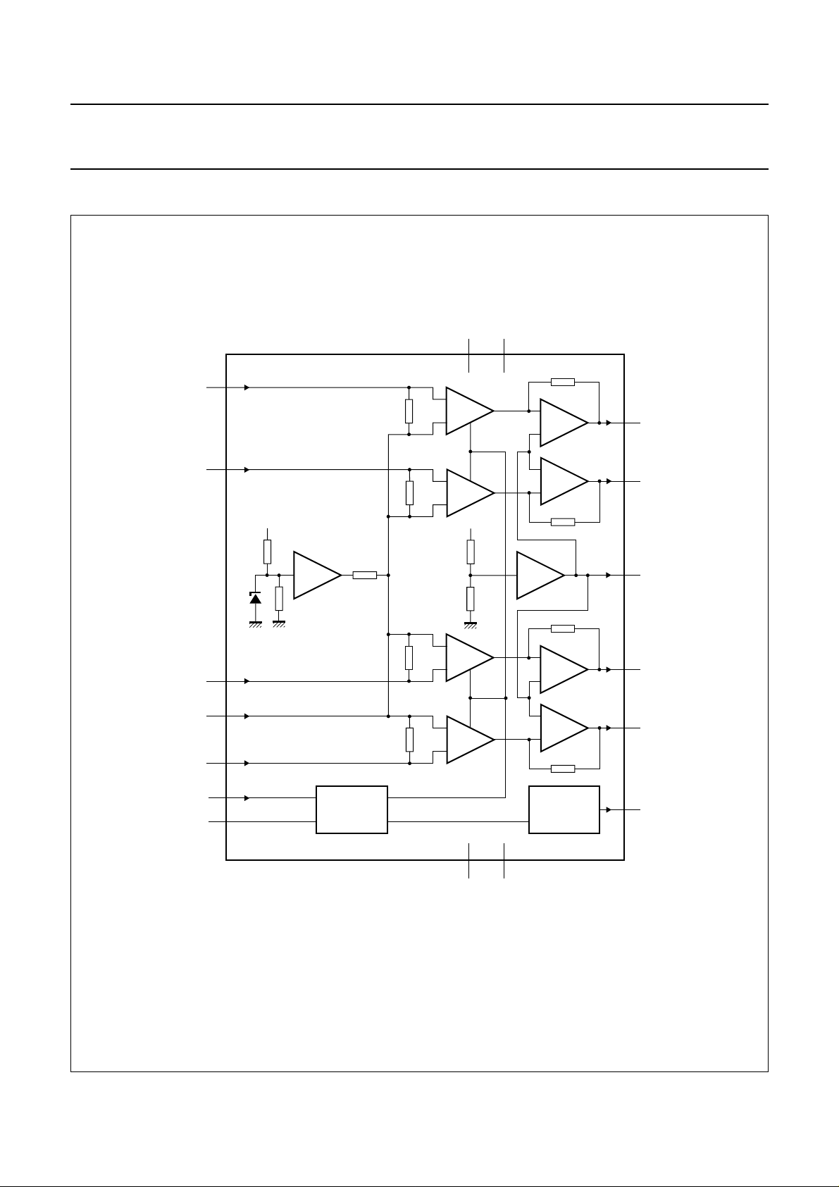
BLOCK DIAGRAM
V
P1VP2
handbook, full pagewidth
IN1
7
60
kΩ
TDA8580
3
15
−
V/I
+
45 kΩ
−
OA
+
1
OUT1+
IN2
IN3
IN5
IN4
MUTE
STANDBY
8
+
60
V/I
kΩ
−
V
px
30 kΩ
BUFFER
60
10
12
11
13
5
INTERFACE
kΩ
60
kΩ
V
px
45
kΩ
45
kΩ
−
V/I
+
+
V/I
−
216
PGND1 PGND2
+
OA
−
45 kΩ
BUFFER
45 kΩ
−
OA
+
+
OA
−
45 kΩ
DIAGNOSTIC
4
9
14
17
6
MGE010
OUT2−
BUFFER
OUT3−
OUT4+
DIAG
Fig.1 Block diagram.
1998 Feb 25 4
Philips Semiconductors Preliminary specification
Multi-purpose power amplifier TDA8580
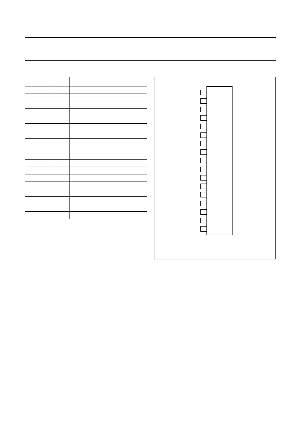
PINNING
SYMBOL PIN DESCRIPTION
OUT1+ 1 non-inverting output 1
PGND1 2 power ground 1
V
P1
3 supply voltage 1
OUT2− 4 inverting output 2
STANDBY 5 ‘standby’/‘mute’/‘on’ selection
DIAG 6 diagnostic output
IN1 7 input 1
IN2 8 input 2
BUFFER 9 buffer output
(single-ended output buffer)
IN3 10 input 3
IN4 11 input 4
IN5 12 input 5; signal ground capacitor
MUTE 13 ‘mute’/‘on’ selection
OUT3− 14 inverting output 3
V
P2
15 supply voltage 2
PGND2 16 power ground 2
OUT4+ 17 non-inverting output 4
handbook, halfpage
STANDBY
OUT1+
PGND1
V
P1
OUT2−
DIAG
IN1
IN2
BUFFER
IN3
IN4
IN5
MUTE
OUT3−
V
P2
PGND2
OUT4+
1
2
3
4
5
6
7
8
9
10
11
12
13
14
15
16
17
TDA8580
MGE009
1998 Feb 25 5
Fig.2 Pin configuration.

Philips Semiconductors Preliminary specification
Multi-purpose power amplifier TDA8580
FUNCTIONAL DESCRIPTION
The TDA8580 is a multi-purpose power amplifier with four
amplifiers which can be connected in the following
configurations with high output power and low distortion (at
minimum quiescent current);
• Dual bridge-tied load (BTL) amplifiers
• Quad single-ended amplifiers
• Dual single-ended amplifiers and one bridge-tied load
amplifier.
The amplifier can be switched on (play or ‘mute’) and off
(‘standby’) by the MUTE and STANDBY pins (for
interfacing directly with a microcontroller). One-pin
operation is also possible by applying a voltage greater
than 8 V to the ‘standby’/’mute’/’on’ selection pin (pin 5) to
switch the amplifier in ‘on’ mode.
Special attention is given to the dynamic behaviour as
follows:
• Noise suppression during engine start.
• No plops when switching from ‘standby’ to ‘on’.
• Slow offset change between ‘mute’ and ‘on’ (controlled
by MUTE and STANDBY pins).
• Low noise levels, which are independent of the supply
voltage.
Protections are included to avoid the IC being damaged at:
• Over temperature: T > 150 °C.
• Short-circuit of the output pin(s) to ground or supply rail.
When short-circuited, the power dissipation is limited.
• A missing-current limiter which limits the maximum short
circuit output current to PGND or V
pins to 1 A.
P
The dissipation and speaker current will be minimized
because the short-circuited amplifier is switched off. The
chip temperature is limited by the temperature
protection.
• ESD protection (Human Body Model 3000 V, Machine
Model 300 V).
• Energy handling. A DC voltage of 6 V can be connected
to the output of any amplifier while the supply pins are
short-circuited to ground. No high DC current will flow
from the supply pins of the amplifier.
Diagnostics are available for the following conditions
(see Figs 4 to 7).
• Amplifier in ‘mute’
• Chip temperature greater than 145 °C
• Distortion over 2% due to clipping
• Short-circuit protection active.
LIMITING VALUES
In accordance with the Absolute Maximum Rating System (IEC 134).
SYMBOL PARAMETER CONDITIONS MIN. MAX. UNIT
V
P
supply voltage operating 8 28 V
load dump protected;
− 45 V
see Fig.3
V
DIAG
I
OSM
I
ORM
V
rev
V
sc
P
tot
T
j
T
stg
T
amb
voltage on diagnostic pin − 18 V
non-repetitive peak output current − 6A
repetitive peak output current − 4.5 A
reverse polarity voltage − 6V
AC and DC short-circuit voltage of output
pins across loads and to ground or supply
pins
no external series
resistor in supply line;
note 1
− 24 V
total power dissipation − 75 W
junction temperature − 150 °C
storage temperature −55 +150 °C
operating ambient temperature −40 +150 °C
Note
1. The maximum supply voltage under short circuit conditions is 28 V with an additional resistor in the supply line of
tbf Ω.
1998 Feb 25 6
 Loading...