

Philips TDA8578T, TDA8578 Datasheet

INTEGRATED CIRCUITS
DATA SH EET
TDA8578
Dual common-mode rejection
differential line receiver
Product specification
Supersedes data of November 1993
File under Integrated Circuits, IC01
1995 Dec 15

Philips Semiconductors Product specification
Dual common-mode rejection differential
TDA8578
line receiver
FEATURES
• Excellent common-mode rejection up to high
frequencies
• Elimination of source resistance in the common-mode
rejection
• Few external components
• High supply voltage ripple rejection
• Low noise
• Low distortion
• Protected against electrostatic discharge
• AC and DC short circuit safe to ground and V
CC
• Fast DC settling.
QUICK REFERENCE DATA
SYMBOL PARAMETER CONDITIONS MIN. TYP. MAX. UNIT
V
CC
I
CC
G
v
supply voltage 5 8.5 18 V
supply current VCC= 8.5 V − 11 14 mA
voltage gain −0.5 0 +0.5 dB
SVRR supply voltage ripple rejection −55 −60 − dB
V
no
Z
input impedance 100 240 − kΩ
i
noise output voltage − 3.7 5 µV
CMRR common-mode rejection ratio R
APPLICATIONS
• Audio
• Car radio.
GENERAL DESCRIPTION
The TDA8578 is a two-channel differential amplifier in a
16 pin DIL or SO package intended to receive line inputs
in audio applications requiring a high-level of
common-mode rejection. The amplifier has a gain of 0 dB
and a low distortion. The device is primarily developed for
those car radio applications where long connections
between signal sources and amplifiers (or boosters) are
necessary and ground noise has to be eliminated.
=0Ω−80 − dB
s
ORDERING INFORMATION
TYPE
NUMBER
NAME DESCRIPTION VERSION
PACKAGE
TDA8578 DIP16 plastic dual in-line package; 16 leads (300 mil); long body SOT38-1
TDA8578T SO16 plastic small outline package; 16 leads; body width 3.9 mm SOT109-1
1995 Dec 15 2
Philips Semiconductors Product specification
Dual common-mode rejection differential
line receiver
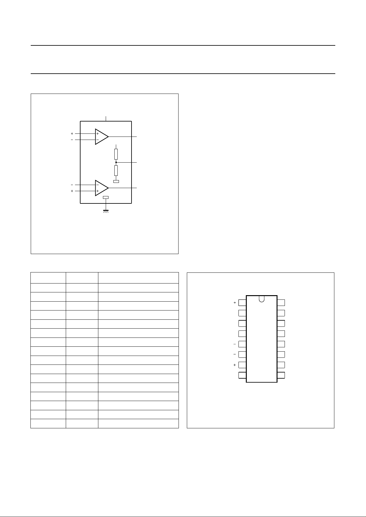
BLOCK DIAGRAM
V
CC
TDA8578
GND
16
12
OUTL
V
CC
8
SVRR
11
OUTR
9
MBD209
INL
INL
INR
INR
1
5
6
7
TDA8578
FUNCTIONAL DESCRIPTION
The TDA8578 contains two identical differential amplifiers
with a voltage gain of 0 dB. The device is intended to
receive line input signals. The device has a very high-level
of common-mode rejection and it eliminates ground noise.
The common-mode rejection keeps constant up to high
frequencies. The gain of the amplifiers is fixed at 0 dB. The
inputs have a high-input impedance and the output stage
is a class AB stage with a low-output impedance. For a
large common-mode rejection also at low frequencies, an
electrolytic input capacitor at the negative input pin is
advised. The input impedance is relative high, this would
result in a large settling time of the DC input voltage.
Therefore a quick charge circuit is included that charges
the input capacitor within 0.2 s.
All input and output pins are protected against high
electrostatic discharge conditions (4000 V, 150 pF, 150 Ω).
Fig.1 Block diagram.
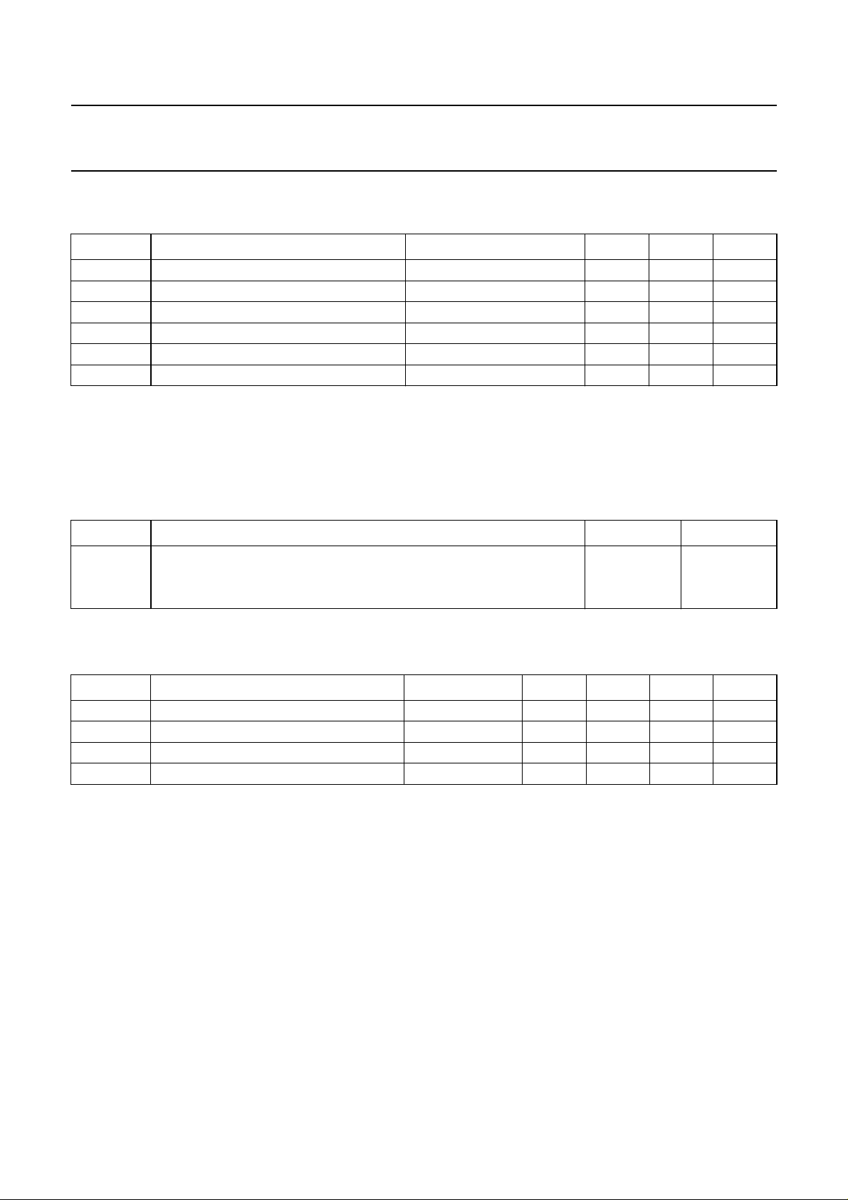
PINNING
SYMBOL PIN DESCRIPTION
INL+ 1 positive input left
n.c. 2 not connected
n.c. 3 not connected
n.c. 4 not connected
INL− 5 negative input left
INR− 6 negative input right
INR+ 7 positive input right
SVRR 8 half supply voltage
GND 9 ground
n.c. 10 not connected
OUTR 11 output right
OUTL 12 output left
n.c. 13 not connected
n.c. 14 not connected
n.c. 15 not connected
V
CC
16 supply voltage
1
INL
2
n.c.
3
n.c.
4
n.c.
INL
INR
INR
SVRR
TDA8578
5
6
7
8
MBD210
Fig.2 Pin configuration.
V
16
CC
15
n.c.
n.c.
14
13
n.c.
OUTL
12
OUTR
11
n.c.
10
GND
9
1995 Dec 15 3
Philips Semiconductors Product specification
Dual common-mode rejection differential
TDA8578
line receiver
LIMITING VALUES
In accordance with the Absolute Maximum Rating System (IEC 134).
SYMBOL PARAMETER CONDITIONS MIN. MAX. UNIT
V
CC
I
ORM
V
sc
T
stg
T
amb
T
j
HANDLING
Inputs and outputs are protected against electrostatic discharges in normal handling. However, to be totally safe, it is
desirable to take normal precautions appropriate to handling integrated circuits.
THERMAL CHARACTERISTICS
SYMBOL PARAMETER VALUE UNIT
R
th j-a
supply voltage operating − 18 V
repetitive peak output current − 40 mA
AC and DC short-circuit safe voltage − 18 V
storage temperature −55 +150 °C
operating ambient temperature −40 +85 °C
junction temperature − +150 °C
thermal resistance from junction to ambient in free air
TDA8578 (DIP16) 75 K/W
TDA8578T (SO16) 120 K/W
DC CHARACTERISTICS
V
= 8.5 V; T
CC
=25°C; in accordance with test circuit (see Fig.3); unless otherwise specified.
amb
SYMBOL PARAMETER CONDITIONS MIN. TYP. MAX. UNIT
V
CC
I
CC
V
O
t
set
supply voltage 5 8.5 18 V
supply current − 11 14 mA
DC output voltage note 1 − 4.3 − V
DC input voltage settling time − 0.2 − s
Note
1. The DC output voltage with respect to ground is approximately 0.5V
CC
.
1995 Dec 15 4
 Loading...