


INTEGRATED CIRCUITS
DATA SH EET
TDA8577
Dual common-mode rejection
differential line receiver
Preliminary specification
File under Integrated Circuits, IC01
Philips Semiconductors
September 1995
Philips Semiconductors Preliminary specification
Dual common-mode rejection differential
TDA8577
line receiver
FEATURES
• Excellent common-mode rejection, up to high
frequencies
• Elimination of source resistance dependency in the
common-mode rejection
• Few external components
• High supply voltage ripple rejection
• Low noise
• Low distortion
• All pins protected against electrostatic discharge
• AC and DC short-circuit safe to ground and V
CC
• Fast DC settling.
QUICK REFERENCE DATA
SYMBOL PARAMETER CONDITIONS MIN. TYP. MAX. UNIT
V
CC
I
CC
G
v
supply voltage 5.0 8.5 18 V
supply current VCC = 8.5 − 11 14 mA
voltage gain −0.5 0 +0.5 dB
SVRR supply voltage ripple rejection 55 60 − dB
V
no
| input impedance 100 240 − kΩ
|Z
i
CMRR common-mode rejection ratio R
noise output voltage − 3.7 5.0 µV
= 0 Ω−80 − dB
s
GENERAL DESCRIPTION
The TDA8577 is a two channel differential amplifier with
0 dB gain and low distortion. The device has been
primarily developed for car radio applications where long
connections between signal sources and amplifiers (or
boosters) are necessary and where ground noise has to be
eliminated. The device is intended to be used to receive
line inputs in audio applications that require a high level of
common-mode rejection. The device is contained in a
9-pin single in-line package.
ORDERING INFORMATION
EXTENDED TYPE
NUMBER
TDA8577 9 SIL9 plastic SOT142
PACKAGE
PINS PIN POSITION MATERIAL CODE
September 1995 2
Philips Semiconductors Preliminary specification
Dual common-mode rejection differential
line receiver
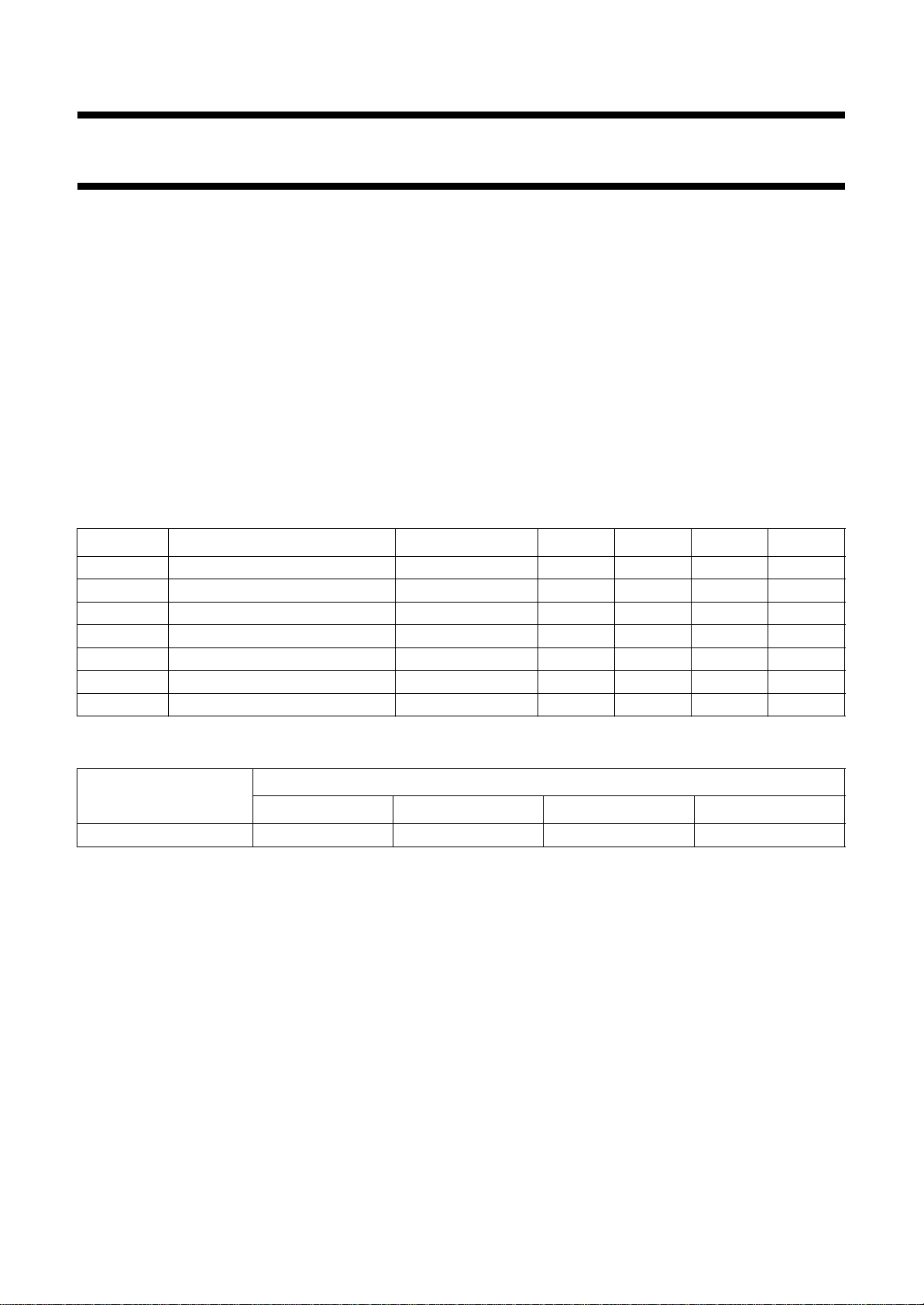
BLOCK DIAGRAM
V
CC
TDA8577
GND
9
8
OUTL
V
CC
5
SVRR
7
OUTR
6
MBD226
INL
INL
INR
INR
1
2
3
4
TDA8577
FUNCTIONAL DESCRIPTION
The TDA8577 contains two identical differential amplifiers
with a voltage gain of 0 dB. The device is intended to
receive line input signals for audio applications. The
TDA8577 has a very high level of common-mode rejection
and thus eliminates ground noise. The common-mode
rejection remains constant up to high frequencies (the
amplifier gain is fixed at 0 dB). The inputs have a high input
impedance. The output stage is a class AB stage with a
low output impedance. For a large common-mode
rejection, also at low frequencies, an electrolytic capacitor
connected to the negative input is advised. Because the
input impedance is relatively high, this results in a large
settling time of the DC input voltage. Therefore a
quick-charge circuit is included to charge the input
capacitor within 0.2 seconds.
All input and output pins are protected against high
electrostatic discharge conditions (4000 V, 150 pF, 150 Ω).
Fig.1 Block diagram.
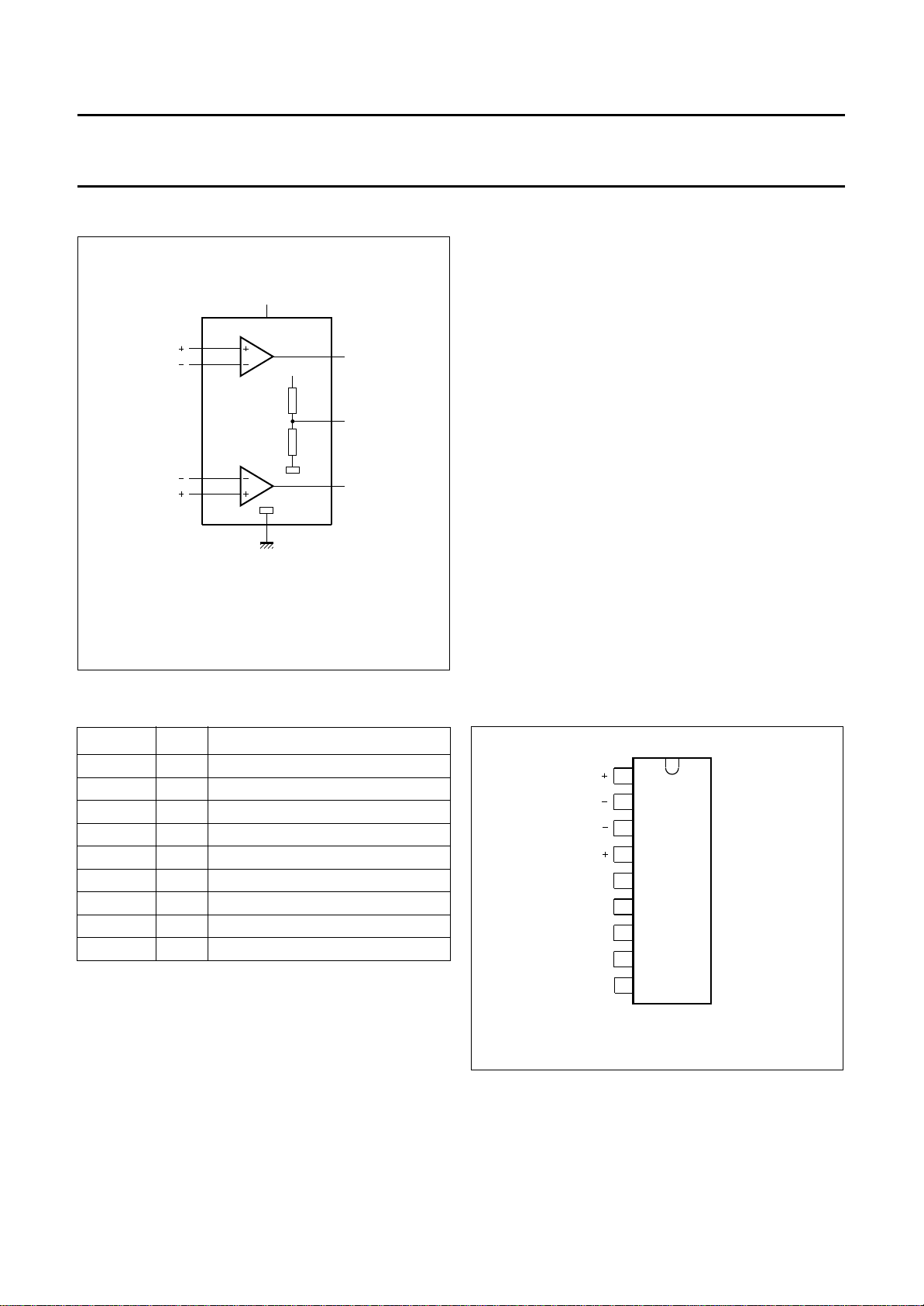
PINNING
SYMBOL PIN DESCRIPTION
INL+ 1 positive input left
INL− 2 negative input left
INR− 3 negative input right
INR+ 4 positive input right
SVRR 5 half supply voltage
GND 6 ground
OUTR 7 output right
OUTL 8 output left
V
CC
9 supply voltage
INL
1
INL
2
INR
3
4
INR
5
SVRR
GND
OUTR
OUTL
V
CC
TDA8577
6
7
8
9
MBD227
Fig.2 Pin configuration.
September 1995 3
Philips Semiconductors Preliminary specification
Dual common-mode rejection differential
TDA8577
line receiver
LIMITING VALUES
In accordance with the Absolute Maximum Rating System (IEC 134).
SYMBOL PARAMETER CONDITIONS MIN. MAX. UNIT
V
CC
I
ORM
V
sc
T
stg
T
amb
T
j
THERMAL RESISTANCE
SYMBOL PARAMETER THERMAL RESISTANCE
R
th j-a
supply voltage operating − 18 V
repetitive peak output current − 40 mA
AC and DC short-circuit safe voltage − 18 V
storage temperature −55 +150 °C
operating ambient temperature −40 +85 °C
maximum junction temperature − +150 °C
from junction to ambient in free air 80 K/W
September 1995 4
 Loading...