

Philips TDA8575T, TDA8575 Datasheet

INTEGRATED CIRCUITS
DATA SH EET
TDA8575
Ground noise isolation amplifier
Preliminary specification
File under Integrated Circuits, IC01
1996 Jul 29

Philips Semiconductors Preliminary specification
Ground noise isolation amplifier TDA8575
FEATURES
• High common mode rejection up to high frequencies
• Reduced dependency of common mode rejection on
source resistance
• Low distortion
• Low noise
• AC and DC short-circuit safe
• Few external components
• ESD protected on all pins.
GENERAL DESCRIPTION
The TDA8575(T) is a two channel amplifier with differential
input and single-ended output for use in car audio
applications. The differential amplifier has a gain of 0 dB,
a low distortion and a high common mode rejection. The
TDA8575T comes in a 16 pin SO package and TDA8575
comes in a 16 pin DIP package.
The TDA8575(T) is developed for those car audio
applications where long connections between signal
sources and amplifiers (or boosters) are necessary and
ground noise has to be eliminated.
QUICK REFERENCE DATA
SYMBOL PARAMETER CONDITIONS MIN. TYP. MAX. UNIT
V
CC
I
CC
G
v
V
o(rms)(max)
supply voltage 5 8.5 18 V
supply current VCC= 8.5 V − 12.6 15 mA
voltage gain −0.5 0 +0.5 dB
maximum output voltage (RMS value) THD = 0.1% − 1.7 − V
SVRR supply voltage ripple rejection 55 60 − dB
CMRR common mode rejection ratio Rs= 0 Ω − 80 − dB
THD total harmonic distortion V
V
no
noise output voltage − 3.7 5 µV
= 1 V; f = 1 kHz − 0.005 − %
o(rms)
Zi input impedance − 108 − kΩ
Zo output impedance − − 10 Ω
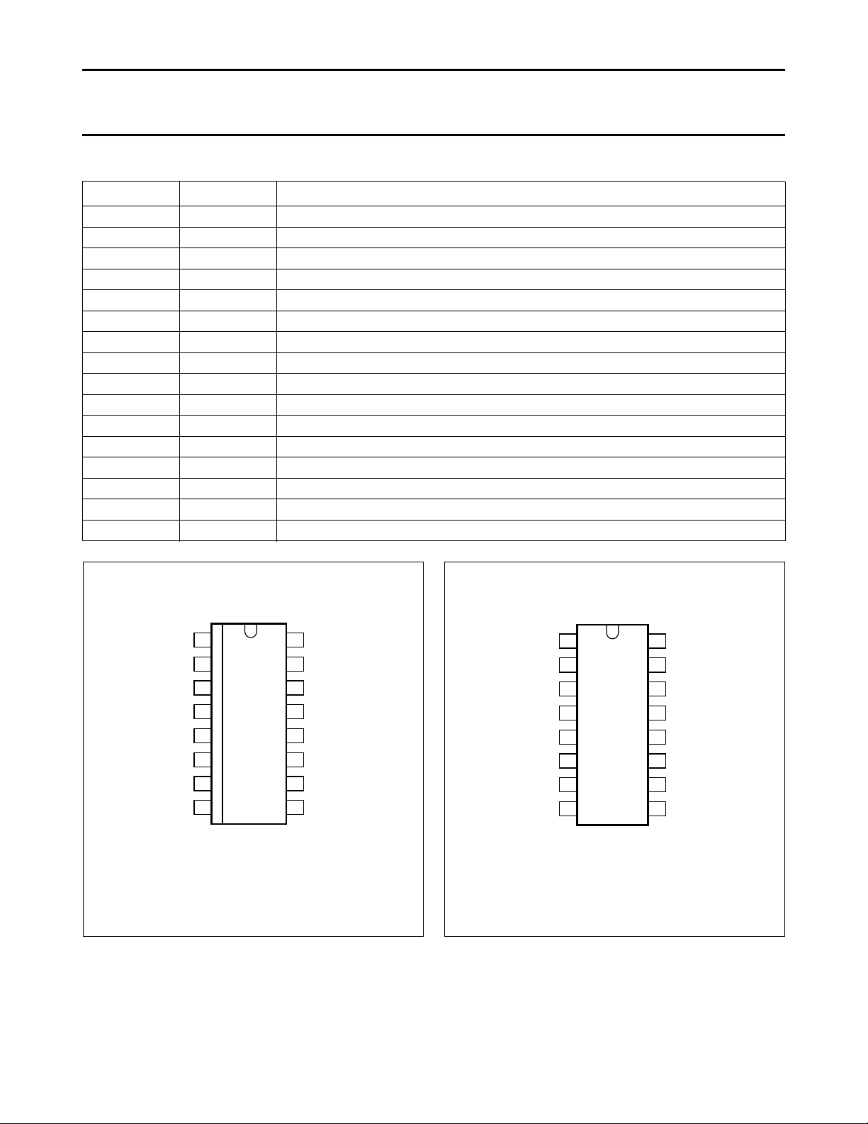
ORDERING INFORMATION
TYPE
NUMBER
TDA8575T SO16
TDA8575 DIP16
NAME DESCRIPTION VERSION
plastic small outline package; 16 leads; body width 3.9 mm SOT109-1
plastic dual in-line package; 16 leads (300 mil); long body SOT38-1
1996 Jul 29 2
PACKAGE
Philips Semiconductors Preliminary specification
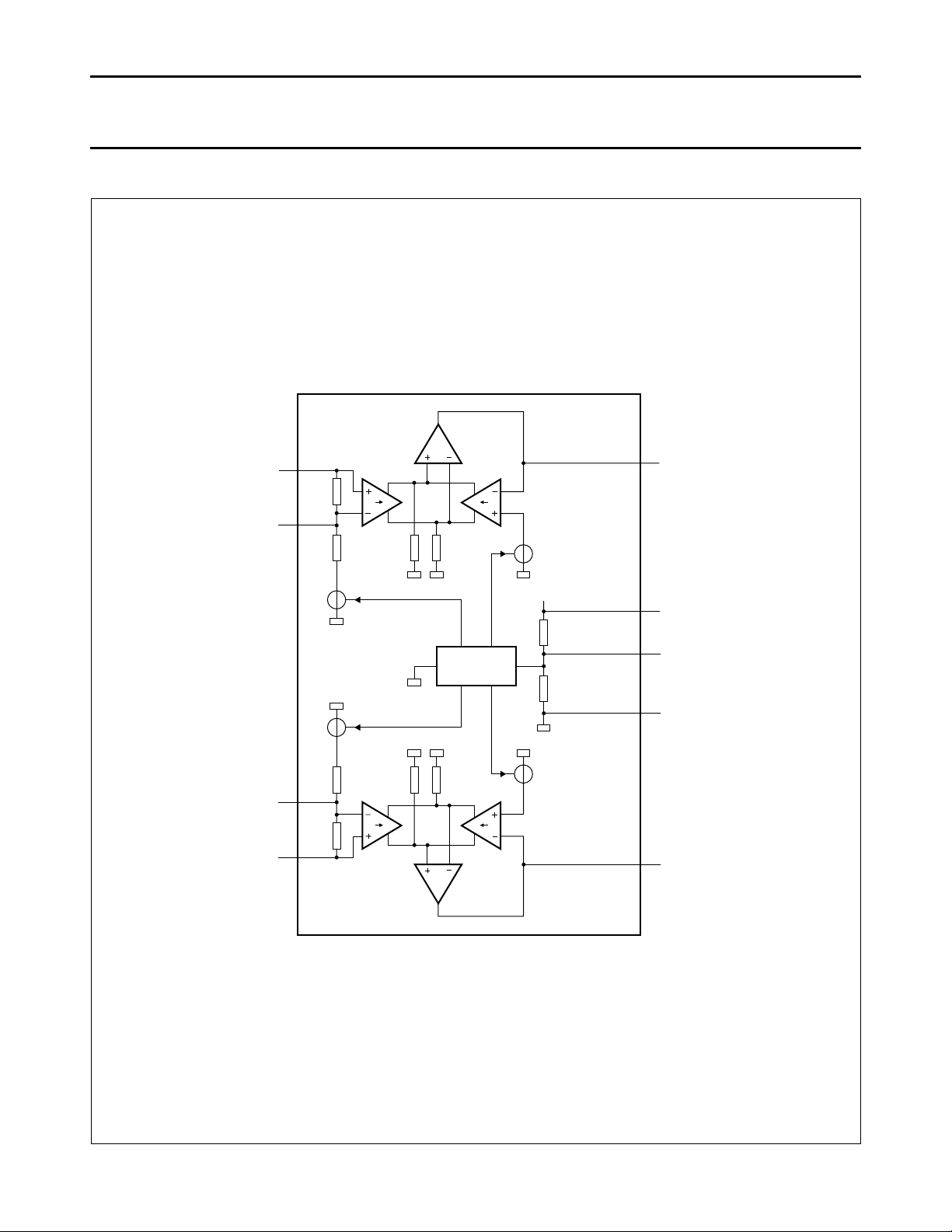
Fig.1 Block diagram.
handbook, full pagewidth
MGE829
360 kΩ
16
0.5(VCC − 0.7) + 0.7
0.5(VCC − 0.7) + 0.7
V
CC
V
CC
9
GND
8
SVRR
12
OUTL
11
OUTR
0.68(VCC − 0.7) + 0.7
0.68(VCC − 0.7) + 0.7
REFERENCE
360 kΩ
108
kΩ
108
kΩ
TDA8575(T)
1
5
6
INR+
INR−
7
INL+
INL−
V I
I V
I V
V I
BLOCK DIAGRAM
Ground noise isolation amplifier TDA8575
1996 Jul 29 3
Philips Semiconductors Preliminary specification
Fig.2 Pin configuration TDA8575T.
handbook, halfpage
TDA8575T
MGE828
1
2
3
4
5
6
7
8
16
15
14
13
12
11
10
9
INL+
n.c.
n.c.
n.c.
INL−
INR−
INR+
SVRR
GND
n.c.
OUTR
OUTL
n.c.
n.c.
n.c.
V
CC
handbook, halfpage
TDA8575
MGE827
1
2
3
4
5
6
7
8
16
15
14
13
12
11
10
9
INL+
n.c.
n.c.
n.c.
INL−
INR−
INR+
SVRR
GND
n.c.
OUTR
OUTL
n.c.
n.c.
n.c.
V
CC
Fig.3 Pin configuration TDA8575.
Ground noise isolation amplifier TDA8575
PINNING
SYMBOL PIN DESCRIPTION
INL+ 1 positive input left
n.c. 2 not connected
n.c. 3 not connected
n.c. 4 not connected
INL− 5 negative input left
INR− 6 negative input right
INR+ 7 positive input right
SVRR 8 supply voltage ripple rejection
GND 9 ground
n.c. 10 not connected
OUTR 11 output voltage right channel
OUTL 12 output voltage left channel
n.c. 13 not connected
n.c. 14 not connected
n.c. 15 not connected
V
CC
16 supply voltage
1996 Jul 29 4
Philips Semiconductors Preliminary specification
Ω
2
-------------------
× 22 µF× 20s= =
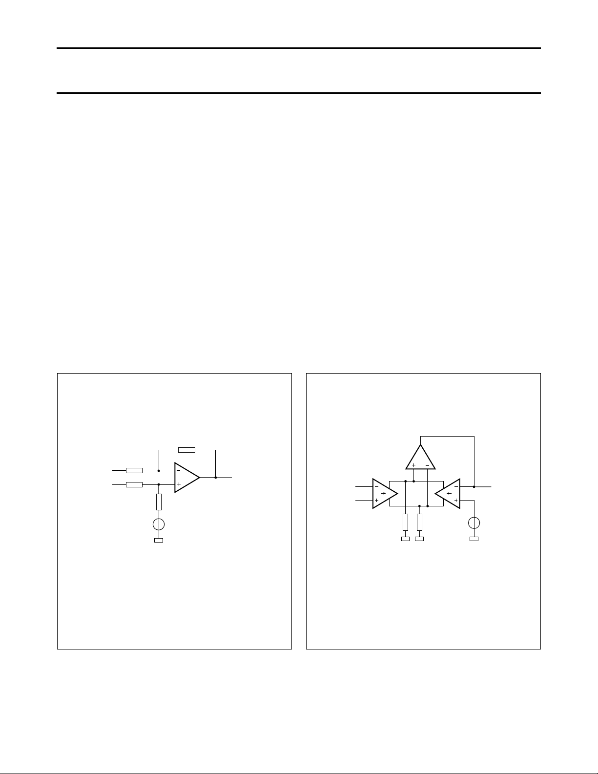
Fig.4 Conventional system.
handbook, halfpage
MGE830
V
o
V
i
0.5 V
CC
Fig.5 New system using V → I converters.
handbook, halfpage
0.5 V
CC
V
o
V
i
V I
I V
MGE831
Ground noise isolation amplifier TDA8575
FUNCTIONAL DESCRIPTION
System description
To enable a high common mode rejection a new system
setup is used. The voltage to current converter, referred to
as V → I in the block diagram of Fig.1, replaces the
resistors that can be seen in the conventional system
solution.
Both systems are shown in Figs 4 and 5. In the
conventional system the common mode rejection is limited
by the matching properties of the resistors resulting in a
CMRR of 60 dB maximum. Using the new system setup a
CMRR of 80 dB is achieved.
Power on
In Fig.6 the preferred input capacitor values are shown.
If the capacitor C2 = 22 µF connected to the IN- inputs had
to be charged by the 0.5Vcc voltage source a charge time
of would be required.5τ 5
360 k
This is inconvenient for most applications and therefore
the TDA8575(T) is equipped with a quick charge circuit.
On power-on the quick charge circuit charges the
capacitor C2 connected to the IN- pins. The quick charge
circuit consists of a voltage buffer and a control circuit
(referred to as ‘reference and power check’ in Fig.6) that
monitors the supply voltage VCC. If the supply voltage rises
more than ≈ 2 V the voltage buffer is switched on.
After charging C2 the voltage buffer is switched off.
The charge time of C2 will equal the charge time of C4, the
SVRR capacitor.
1996 Jul 29 5
 Loading...