

Philips TDA8574T-N1 Datasheet

DATA SH EET
Product specification
Supersedes data of 1997 Feb 26
File under Integrated Circuits, IC01
1998 Oct 16
INTEGRATED CIRCUITS
TDA8574
Class-H high-output voltage level
line driver
1998 Oct 16 2
Philips Semiconductors Product specification
Class-H high-output voltage level line
driver
TDA8574
FEATURES
• Output voltage swing larger than supply voltage
• High supply voltage ripple rejection
• Low distortion
• Low noise
• ESD protected on all pins.
GENERAL DESCRIPTION
The TDA8574(T) is a two channel class-H high-output
voltage line driver for use in car audio applications.
The line driver behaves as a non-inverting amplifier with a
gain of 8 dB and a single-ended output. Due to the class-H
voltage lifting principle the voltage swing over the load is
more than the supply voltage. With a supply voltage of 9 V
the output voltage swing over the load will be
14 V (peak-to-peak).
The TDA8574 is available in a DIP16 package and the
TDA8574T in a SO16 package.
Line drivers are necessary in car audio systems in which
the power amplifiers are driven by long cables.
The signal-to-noise ratio of these car audio systems is
improved by using the TDA8574(T) class-H high-output
level line driver. The high-output level of TDA8574(T)
enables a reduction of the gain of the power amplifier
resulting in an improvement of the power amplifier
performance.
QUICK REFERENCE DATA
ORDERING INFORMATION
SYMBOL PARAMETER CONDITIONS MIN. TYP. MAX. UNIT
V
CC
supply voltage 6 9 12 V
I
CC
supply current VCC=9V − 813mA
G
v
voltage gain 7.5 8 8.5 dB
V
o(rms)
maximal output voltage (RMS value) THD = 0.1% 5.0 5.2 − V
SVRR supply voltage ripple rejection 50 65 − dB
THD total harmonic distortion V
o(rms)
= 3 V; f = 1 kHz − 0.003 − %
V
no
noise output voltage − 5 −µV
Z
o
output impedance −−10 Ω
TYPE
NUMBER
PACKAGE
NAME DESCRIPTION VERSION
TDA8574T SO16 plastic small outline package; 16 leads; body width 7.5 mm SOT162-1
TDA8574 DIP16 plastic dual in-line package; 16 leads (300 mil) SOT38-4
1998 Oct 16 3
Philips Semiconductors Product specification
Class-H high-output voltage level line
driver
TDA8574
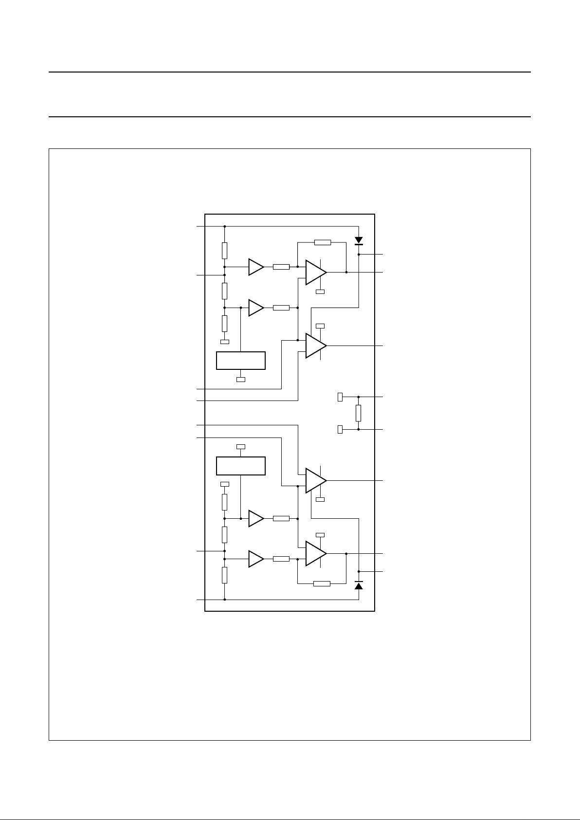
BLOCK DIAGRAM
Fig.1 Block diagram.
handbook, full pagewidth
MGE668
24 kΩ
30 kΩ
5 Ω
36 kΩ
36 kΩ
30 kΩ
24 kΩ
REFERENCE
REFERENCE
LIFT
AMP.
LIFT
AMP.
SIGNAL
AMP.
SIGNAL
AMP.
TDA8574(T)
V
CCL
V
CCL
V
CCR
V
CCR
V
CCL
V
CCR
3
1
BUFFER
BUFFER
BUFFER
BUFFER
CL+
CL−
CR+
CR−
OUTL
13
14
11
12
10
9
6
INR
INMR
INML
INL
SVRL
8
15
16
LGND
RGND
OUTR
2
4
5
7
SVRR
+
+
−
+
−
−
+
−
1998 Oct 16 4
Philips Semiconductors Product specification
Class-H high-output voltage level line
driver
TDA8574
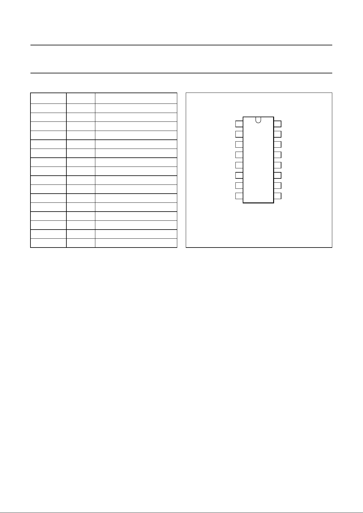
PINNING
SYMBOL PIN DESCRIPTION
V
CCL
1 supply voltage left channel
INL 2 input voltage left channel
SVRL 3 SVRR left channel
INML 4 inverting input left channel
INMR 5 inverting input right channel
SVRR 6 SVRR right channel
INR 7 input voltage right channel
V
CCR
8 supply voltage right channel
CR+ 9 lift capacitor (+) right channel
CR− 10 lift capacitor (−) right channel
RGND 11 ground right channel
OUTR 12 output voltage right channel
OUTL 13 output voltage left channel
LGND 14 ground left channel
CL− 15 lift capacitor (−) left channel
CL+ 16 lift capacitor (+) left channel
Fig.2 Pin configuration.
handbook, halfpage
TDA8574
TDA8574T
MGE667
1
2
3
4
5
6
7
8
16
15
14
13
12
11
10
9
V
CCL
INL
SVRL
INML
INMR
SVRR
INR
V
CCR
CR+
CR−
RGND
OUTR
OUTL
LGND
CL−
CL+
FUNCTIONAL DESCRIPTION
Lift amplifier
The lift amplifier, referred to as LIFT AMP. in Fig.1, is used
as a non-inverting amplifier with a voltage gain of 8 dB set
by an internal feedback network. If the output voltage of
the signal amplifier is low, the external lift capacitor is
recharged by the lift amplifier. As soon as the output
voltage of the signal amplifier increases above 0.87 × V
CC
the lift amplifier switches the voltage of the lift capacitor in
series with the supply voltage VCC. The voltage at the
positive side of the lift capacitor is referred to as lifted
supply voltage.
Signal amplifier
The signal amplifier, referred to as SIGNAL AMP. in Fig.1,
is used as a non-inverting amplifier. The voltage gain G
v
is
set by the feedback resistors according to the formula:
and should be set to 8 dB. The LIFT AMP. and SIG AMP.
must have equal voltage gain Gv. The rail-to-rail output
stage of the signal amplifier uses the lifted supply voltage
to increase the output voltage swing.
G
v
1
R
2
R
1
------ -
+=
The DC output level is set to ≈0.87 × V
CC.
The maximum
peak-to-peak output voltage of the signal amplifier is
calculated with the formula:
Buffers
The buffers prevent loading of the internal voltage divider
network made by a series connection of resistors. For a
good supply voltage ripple rejection this internal voltage
divider network has to be decoupled by an external
capacitor.
Reference
This circuit supplies all currents needed in the device.
V
op p–()max
20.87VCC0.4–()×≈
1998 Oct 16 5
Philips Semiconductors Product specification
Class-H high-output voltage level line
driver
TDA8574
LIMITING VALUES
In accordance with the Absolute Maximum Rating System (IEC 134).
THERMAL CHARACTERISTICS
SYMBOL PARAMETER CONDITIONS MIN. MAX. UNIT
V
CC
supply voltage operating − 12 V
I
ORM
repetitive peak output current − 20 mA
T
stg
storage temperature −55 +150 °C
T
amb
operating ambient temperature −40 +85 °C
T
j
junction temperature − +150 °C
SYMBOL PARAMETER VALUE UNIT
R
th j-a
thermal resistance from junction to ambient in free air
TDA8574 (DIP16) 75 K/W
TDA8574T (SO16) 110 K/W
 Loading...