

Philips TDA8569Q Datasheet

INTEGRATED CIRCUITS
DATA SH EET
TDA8569Q
4 × 25 W BTL quad car radio power
amplifier
Preliminary specification
File under Integrated Circuits, IC01
1997 Mar 27

Philips Semiconductors Preliminary specification
4 × 25 W BTL quad car radio power
amplifier
FEATURES
• Capable of driving 2 Ω loads
• Requires very few external components
• High output power
• Low output offset voltage
• Fixed gain
• Diagnostic facility (distortion, short-circuit and
temperature pre-warning)
• Good ripple rejection
• Mode select switch (operating, mute and standby)
• Load dump protection
• Short-circuit safe to ground and to V
load
• Low power dissipation in any short-circuit condition
• Thermally protected
• Reverse polarity safe
and across the
P
TDA8569Q
• Electrostatic discharge protection
• No switch-on/switch-off plop
• Flexible leads
• Low thermal resistance
• Pin compatible with the TDA8567Q.
GENERAL DESCRIPTION
The TDA8569Q is an integrated class-B output amplifier in
a 23-lead Single-In-Line (SIL) plastic power package.
It contains four amplifiers in BTL configuration, each with a
gain of 26 dB. The output power is 4 × 25 W in a 4 Ω load.
APPLICA TIONS
• The device is primarily developed for car radio
applications.
QUICK REFERENCE DATA
SYMBOL PARAMETER CONDITIONS MIN. TYP. MAX. UNIT
V
P
I
ORM
I
q(tot)
I
stb
I
sw
input impedance 25 30 − kΩ
Z
i
P
o
SVRR supply voltage ripple rejection R
α
cs
G
v
V
n(o)
∆V
DC output offset voltage −−150 mV
O
operating supply voltage 6 14.4 18 V
repetitive peak output current −−7.5 A
total quiescent current − 230 − mA
standby current − 0.2 100 µA
switch-on current −−80 µA
output power THD = 10% − 25 − W
=0Ω−60 − dB
s
channel separation Rs=10kΩ−50 − dB
closed loop voltage gain 25 26 27 dB
noise output voltage Rs=0Ω−−120 µV
ORDERING INFORMATION
TYPE
NUMBER
NAME DESCRIPTION VERSION
PACKAGE
TDA8569Q DBS23P plastic DIL-bent-SIL power package; 23 leads (straight lead length 3.2 mm) SOT411-1
1997 Mar 27 2
Philips Semiconductors Preliminary specification
4 × 25 W BTL quad car radio power
amplifier
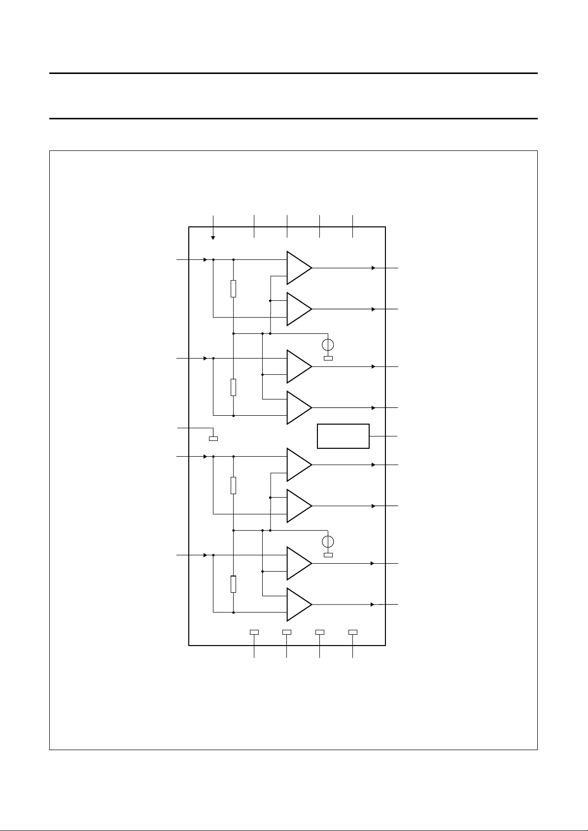
BLOCK DIAGRAM
handbook, full pagewidth
IN1
IN2
SGND
IN3
MODE
10
11
12
13
V
30 kΩ
30 kΩ
TDA8569Q
30 kΩ
P1
TDA8569Q
V
P2
V
+
P3
V
P4
23168115
2
OUT1+
−
+
4
OUT1−
−
V
ref
+
7
OUT2+
−
+
5
OUT2−
−
9
DIAGNOSTIC
+
V
DIAG
17
OUT3+
−
+
19
OUT3−
−
14
IN4
30 kΩ
PGND1 PGND2 PGND3 PGND4
Fig.1 Block diagram.
1997 Mar 27 3
V
ref
+
22
OUT4+
−
+
20
OUT4−
−
211863
MBK010
Philips Semiconductors Preliminary specification
4 × 25 W BTL quad car radio power
amplifier
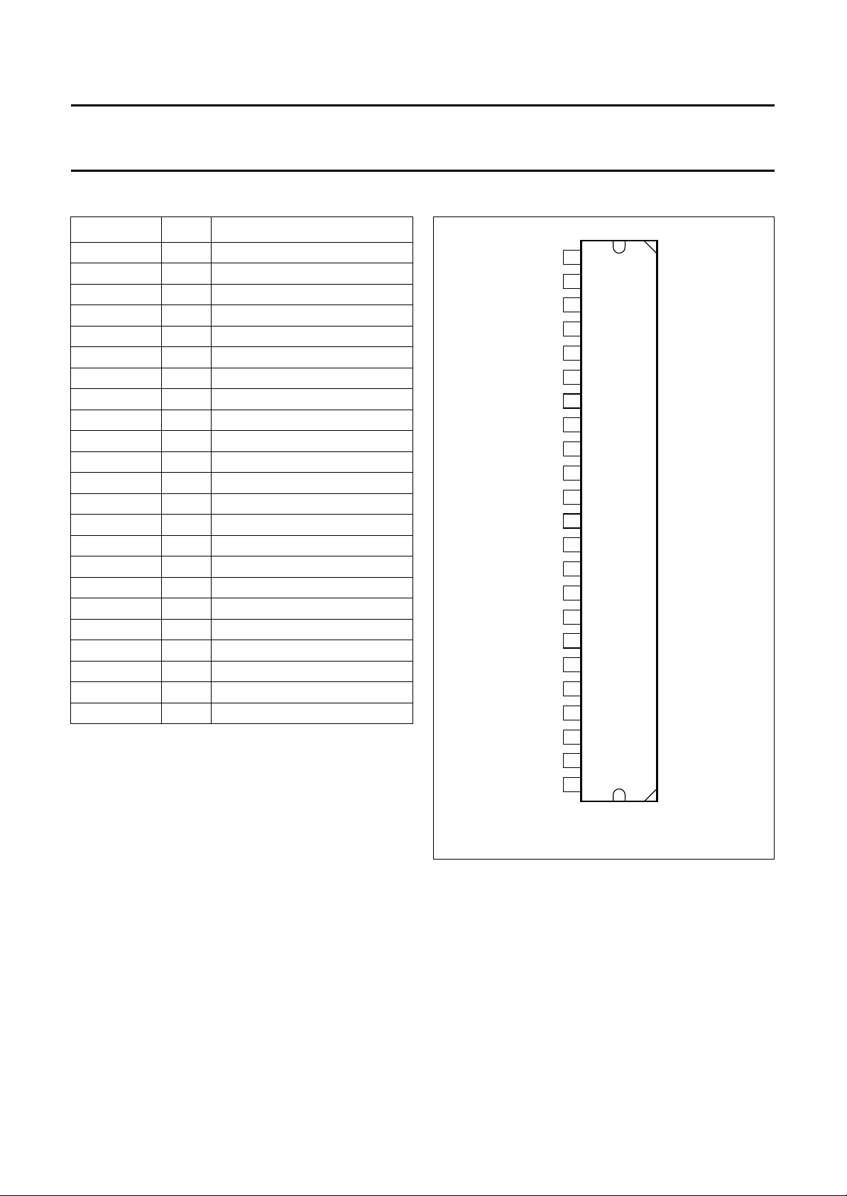
PINNING
SYMBOL PIN DESCRIPTION
V
P1
OUT1+ 2 output 1+
PGND1 3 power ground 1
OUT1− 4 output 1−
OUT2− 5 output 2−
PGND2 6 power ground 2
OUT2+ 7 output 2+
V
P2
V
DIAG
IN1 10 input 1
IN2 11 input 2
SGND 12 signal ground
IN3 13 input 3
IN4 14 input 4
MODE 15 mode select switch input
V
P3
OUT3+ 17 output 3+
PGND3 18 power ground 3
OUT3− 19 output 3−
OUT4− 20 output 4−
PGND4 21 power ground 4
OUT4+ 22 output 4+
V
P4
1 supply voltage 1
8 supply voltage 2
9 diagnostic output
16 supply voltage 3
23 supply voltage 4
handbook, halfpage
V
P1
OUT1+
PGND1
OUT1−
OUT2−
PGND2
OUT2+
V
P2
V
DIAG
IN1
IN2
SGND
IN3
IN4
MODE
V
P3
OUT3+
PGND3
OUT3−
OUT4−
PGND4
OUT4+
V
P4
1
2
3
4
5
6
7
8
9
10
11
TDA8569Q
12
13
14
15
16
17
18
19
20
21
22
23
TDA8569Q
MBK009
1997 Mar 27 4
Fig.2 Pin configuration.

Philips Semiconductors Preliminary specification
4 × 25 W BTL quad car radio power
amplifier
FUNCTIONAL DESCRIPTION
The TDA8569Q contains four identical amplifiers which
can be used for bridge applications. The gain of each
amplifier is fixed at 26 dB.
Mode select switch (pin 15)
• Standby: low supply current (<100 µA)
• Mute: input signal suppressed
• Operating: normal on condition.
Since this pin has a low input current (<80 µA), a low cost
supply switch can be applied.
To avoid switch-on plops, it is advised to keep the amplifier
in the mute mode during ≥150 ms (charging of the input
capacitors at pins 10, 11, 13 and 14).
This can be realized by:
• Microprocessor control
• External timing circuit (see Fig.3).
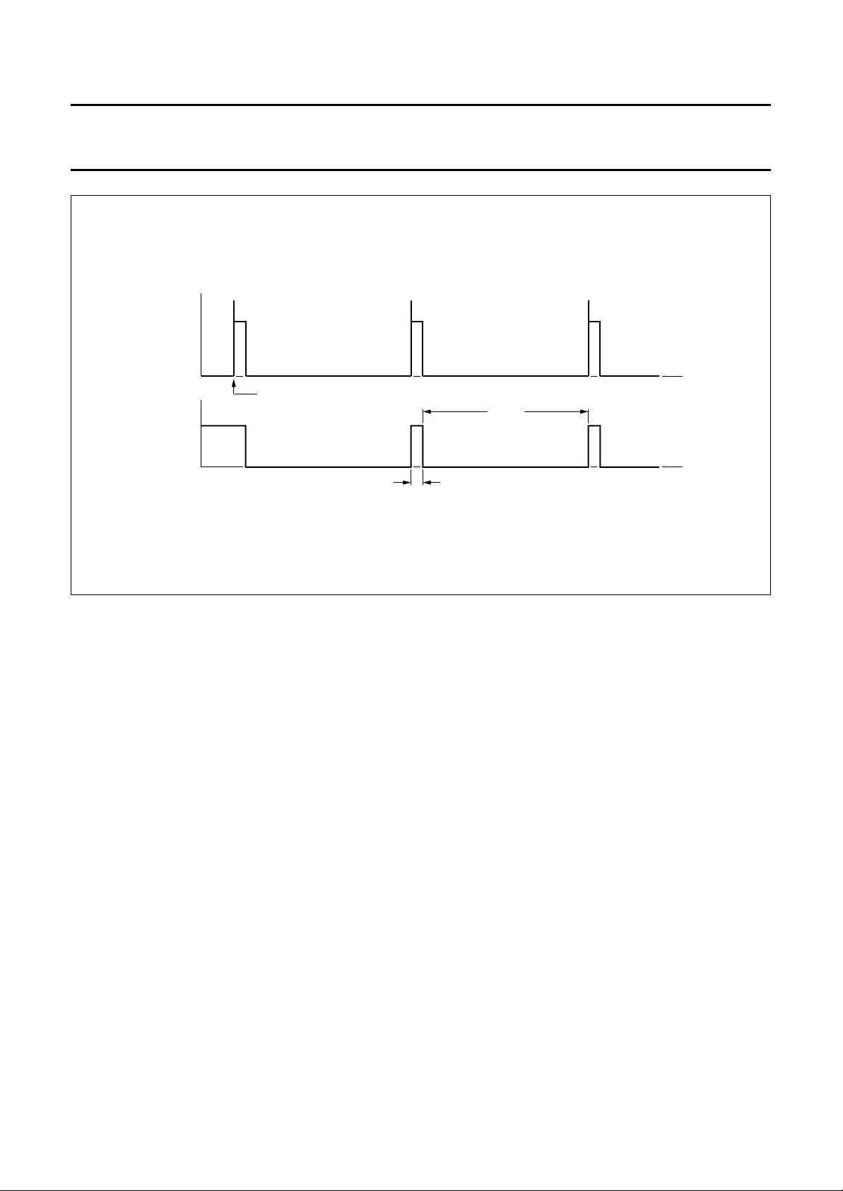
Diagnostic output (pin 9)
YNAMIC DISTORTION DETECTOR (DDD)
D
At the onset of clipping of one or more output stages, the
dynamic distortion detector becomes active and pin 9
goes LOW. This information can be used to drive a sound
processor or DC volume control to attenuate the input
signal and so limit the distortion. The output level of pin 9
is independent of the number of channels that are clipping
(see Fig.4).
TDA8569Q
HORT-CIRCUIT DIAGNOSTIC
S
When a short-circuit occurs at one or more outputs to
ground or to the supply voltage, the output stages are
switched off until the short-circuit is removed and the
device is switched on again, with a delay of approximately
10 ms after removal of the short-circuit. During this
short-circuit condition, pin 9 is continuously LOW.
When a short-circuit occurs across the load of one or more
channels, the output stages are switched off during
approximately 10 ms. After that time it is checked during
approximately 50 µs to determine whether the short-circuit
is still present.
Due to this duty cycle of 50 µs/10 ms the average current
consumption during this short-circuit condition is very low.
During this short-circuit condition, pin 9 is LOW for 10 ms
and HIGH for 50 µs (see Fig.5). The protection circuits of
all channels are coupled. This means that if a short-circuit
condition occurs in one of the channels, all channels are
switched off. Consequently, the power dissipation in any
short-circuit condition is very low.
EMPERATURE PRE-WARNING
T
When the virtual junction temperature Tvj reaches 145 °C,
pin 9 goes LOW.
PEN COLLECTOR OUTPUTS
O
The diagnostic pin has an open collector output, so more
devices can be tied together. An external pull-up resistor is
needed.
V
handbook, halfpage
P
10 kΩ 10 kΩ
47 µF
mode
select
switch
100 kΩ
MGA708
Fig.3 Mode select switch circuitry.
1997 Mar 27 5
handbook, halfpage
V
V
V
Fig.4 Distortion detector waveform.
o
0
9
P
0
MGG155
t
Philips Semiconductors Preliminary specification
4 × 25 W BTL quad car radio power
amplifier
handbook, full pagewidth
short
circuit
current
V
9
short-circuit over the load
V
P
TDA8569Q
MGG156
t
10 ms
t
50 µs
Fig.5 Short-circuit waveform.
1997 Mar 27 6
 Loading...