

Philips TDA8566TH Datasheet

INTEGRATED CIRCUITS
DATA SH EET
TDA8566TH
2 × 40 W/2 Ω stereo BTL car radio
power amplifier with differential
inputs and diagnostic outputs
Objective specification
File under Integrated Circuits, IC01
2001 Apr 24

Philips Semiconductors Objective specification
2 × 40 W/2 Ω stereo BTL car radio power amplifier
with differential inputs and diagnostic outputs
FEATURES
• Differential inputs
• Very high Common Mode Rejection Ratio (CMRR)
• High common mode input signal handling
• Requires very few external components
• High output power
• 4 and 2 Ω load driving capability
• Low offset voltage at output
• Fixed gain
• Diagnostic facility (distortion, short-circuit and
temperature pre-warning)
• Good ripple rejection
• Mode select switch (operating, mute and standby)
• Load dump protection
• Short-circuit proof to ground, to VP and across the load
• Low power dissipation in any short-circuit condition
• Thermally protected
• Reverse polarity safe
• Protected against electrostatic discharge
• No switch-on/switch-off plops
• Low thermal resistance.
GENERAL DESCRIPTION
The TDA8566TH is an integratedclass-B output amplifier
contained in a 20-lead small outline plastic package. The
device contains 2 amplifiers in a Bridge-Tied Load (BTL)
configuration. The output power is 2 × 25Wina4Ωload
or 2 × 40 W in a 2 Ω load. It has a differential input stage
and 2 diagnostic outputs. The device is primarily
developed for car radio applications.
TDA8566TH
QUICK REFERENCE DATA
SYMBOL PARAMETER CONDITIONS MIN. TYP. MAX. UNIT
V
P
I
ORM
I
q(tot)
I
stb
I
sw
Z
i
P
out
SVRR supply voltage ripple rejection R
α
cs
operating supply voltage 6 14.4 18 V
repetitive peak output current −−7.5 A
total quiescent current − 115 − mA
standby current − 0.1 10 µA
switch-on current −−40 µA
input impedance 100 120 − kΩ
output power RL=4Ω; THD = 10% − 25 − W
=2Ω; THD = 10% − 40 − W
R
L
=0Ω−60 − dB
s
channel separation Rs=10kΩ−50 − dB
CMRR common mode rejection ratio − 75 − dB
G
v
V
n(o)
closed loop voltage gain 25 26 27 dB
noise output voltage Rs=0Ω−−120 µV
ORDERING INFORMATION
TYPE
NUMBER
NAME DESCRIPTION VERSION
PACKAGE
TDA8566TH HSOP20 plastic, heatsink small outline package; 20 leads; low stand-off height SOT418-2
2001 Apr 24 2

Philips Semiconductors Objective specification
2 × 40 W/2 Ω stereo BTL car radio power amplifier
with differential inputs and diagnostic outputs
BLOCK DIAGRAM
handbook, full pagewidth
IN1+
IN1−
n.c.
SGND
IN2+
IN2−
8
9
60
60
kΩ
kΩ
4, 5,
6, 7
V
ref
10
60
60
kΩ
kΩ
2
3
17 14
PGND2 PGND1
2.3
2.3
2.3
2.3
kΩ
kΩ
kΩ
kΩ
standby
switch
V
A
1×
mute
switch
+
−
V
A
+
−
mute
switch
+
−
V
A
+
−
mute
switch
+
−
V
A
+
−
mute
switch
+
−
V
A
+
−
standby
reference
voltage
mute
reference
voltage
C
M
2.3 kΩ
(9×)
C
M
2.3 kΩ
(9×)
C
M
2.3 kΩ
(9×)
C
M
2.3 kΩ
(9×)
TDA8566TH
mute
switch
TDA8566TH
V
V
P2
P1
1912
13
OUT1+
15
OUT1−
20
MODE
11
CLIP
DIAG
MGU358
CLIP
1
DIAG
16
OUT2+
18
OUT2−
Fig.1 Block diagram.
2001 Apr 24 3
Philips Semiconductors Objective specification
2 × 40 W/2 Ω stereo BTL car radio power amplifier
with differential inputs and diagnostic outputs
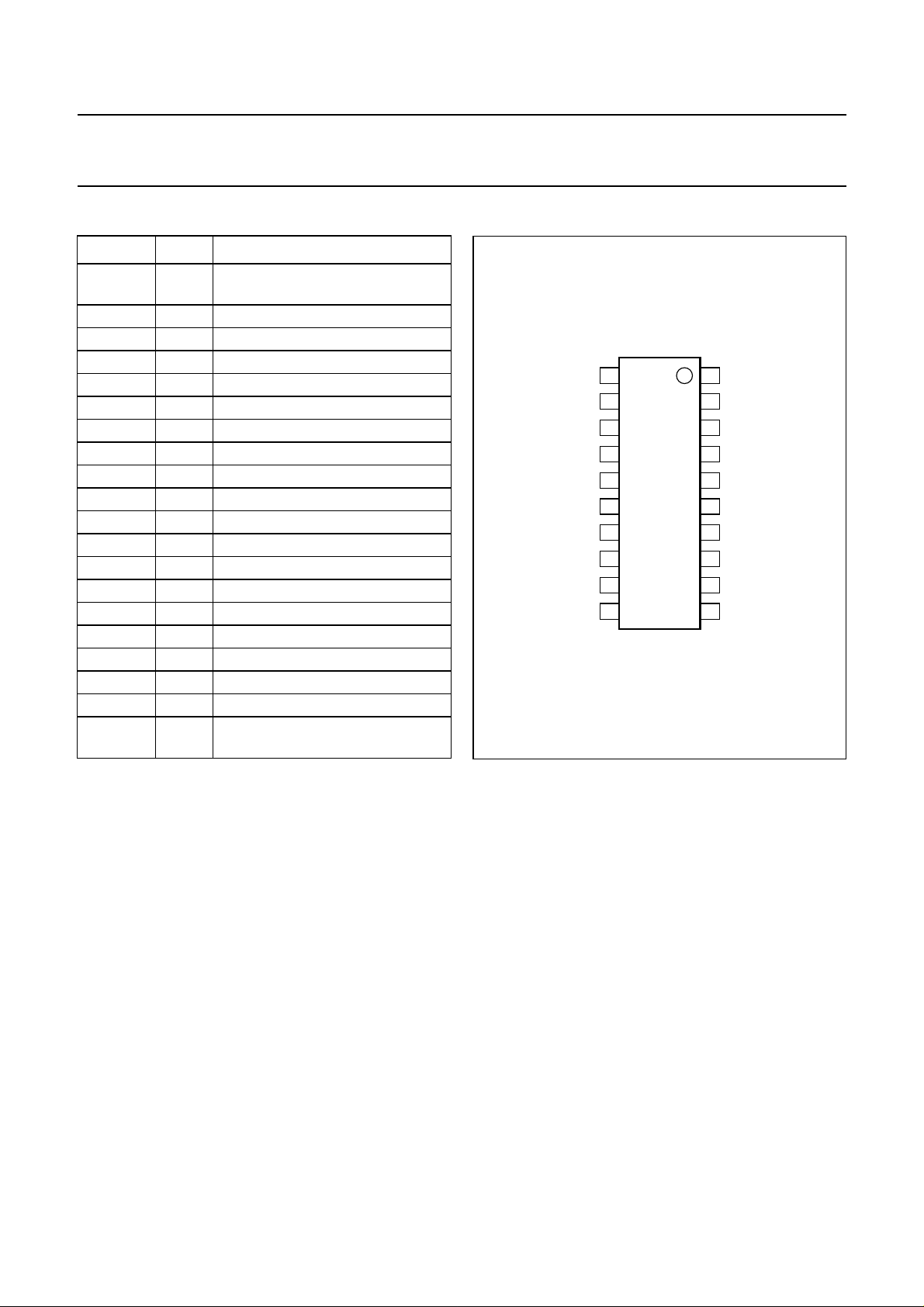
PINNING
SYMBOL PIN DESCRIPTION
DIAG 1 short-circuit and temperature
pre-warning diagnostic output
IN2+ 2 channel 2 input positive
IN2− 3 channel 2 input negative
n.c. 4 not connected
n.c. 5 not connected
n.c. 6 not connected
n.c. 7 not connected
IN1+ 8 channel 1 input positive
IN1− 9 channel 1 input negative
SGND 10 signal ground
CLIP 11 clip detection output
V
P1
12 supply voltage 1
OUT1+ 13 channel 1 output positive
PGND1 14 power ground 1
OUT1− 15 channel 1 output negative
OUT2+ 16 channel 2 output positive
PGND2 17 power ground 2
OUT2− 18 channel 2 output negative
V
P2
19 supply voltage 2
MODE 20 mode select switch input
(standby/mute/operating)
handbook, halfpage
MODE
20
19
V
P2
18
OUT2−
17
PGND2
16
OUT2+
OUT1−
PGND1
OUT1+
V
CLIP
P1
TDA8566TH
15
14
13
12
11
MGU356
Fig.2 Pin configuration.
TDA8566TH
DIAG
1
IN2+
2
IN2−
3
n.c.
4
n.c.
5
n.c.
6
n.c.
7
8
IN1+
IN1−
9
SGND
10
2001 Apr 24 4

Philips Semiconductors Objective specification
2 × 40 W/2 Ω stereo BTL car radio power amplifier
with differential inputs and diagnostic outputs
FUNCTIONAL DESCRIPTION
The TDA8566TH contains 2 identical amplifiers and can
be used for BTL applications. The gain of each amplifier is
fixed at 26 dB. Special features of this device are:
1. Mode select switch
2. Clip detection
3. Short-circuit diagnostic
4. Temperature pre-warning
5. Open-collector diagnostic outputs
6. Differential inputs.
Mode select switch (pin MODE)
• Standby: low supply current
• Mute: input signal suppressed
• Operating: normal on condition.
Since this pin has a very low input current (<40 µA), a low
cost supply switch can be applied. To avoid switch-on
plops,itisadvisabletokeeptheamplifier in the mute mode
for a period of ≥150 ms (charging the input capacitors at
pins IN1+, IN1−, IN2+ and IN2−). This can be realized by
using a microcontroller or by using an external timing
circuit as illustrated in Fig.7.
Clip detection (pin CLIP)
When clipping occurs at one or more output stages, the
dynamic distortion detector becomes active and pin CLIP
goes LOW. This information can be used to drive a sound
processor or a DC volume control to attenuate the input
signal and so limit the level of distortion. The output level
of pin CLIP is independent of the number of channels that
are being clipped. The clip detection circuit is disabled in a
short-circuit condition, so if a fault condition occurs at the
outputs, pin CLIP will remain at a HIGH level. The clip
detection waveforms are illustrated in Fig.3.
Short-circuit diagnostic (pin DIAG)
When a short-circuit occurs at one or more outputs to
ground or to the supply voltage, the output stages are
switched off until the short-circuit is removed and the
device is switched on again (with a delay of approximately
20 ms after the removal of the short-circuit). During this
short-circuit condition, pin DIAG is continuously LOW.
When a short-circuit occurs across the load of one or both
channels, the output stages are switched off for
approximately 20 ms. After that time the load condition is
checked during approximately 50 µs to see whether the
short-circuit is still present. Due to this duty cycle of
50 µs/20 ms the average current consumption during the
short-circuit condition is very low (approximately 40 mA).
During this condition, pin DIAG is LOW for 20 ms and
HIGH for 50 µs; see Fig.4. The power dissipation in any
short-circuit condition is very low.
Temperature pre-warning (pin DIAG)
When the junction temperature (Tvj) reaches 145 °C,
pin DIAG will become continuously LOW.
Open-collector diagnostic outputs
Pins DIAG and CLIP are open-collector outputs, therefore
more devices can be tied together. Pins DIAG and CLIP
can also be tied together. An external pull-up resistor is
required.
Differential inputs
The input stage is a high-impedance fully differential
balanced input stage that is also capable of operating in
a single-ended mode with one of the inputs capacitively
coupled to an audio ground. It should be noted that if a
source resistance is added (input voltage dividers) the
CMRR degrades to lower values.
TDA8566TH
handbook, halfpage
V
V
O
(V)
CLIP
(V)
0
0
MGU357
t (s)
Fig.3 Clip detection waveforms.
2001 Apr 24 5
 Loading...