

Philips TDA8566Q-N2, TDA8566Q-N1 Datasheet

DATA SH EET
Product specification
Supersedes data of 1998 Sep 23
File under Integrated Circuits, IC01
2000 Jan 28
INTEGRATED CIRCUITS
TDA8566Q
2 × 40 W/2 Ω stereo BTL car radio
power amplifier with differential
inputs and diagnostic outputs

2000 Jan 28 2
Philips Semiconductors Product specification
2 × 40 W/2 Ω stereo BTL car radio power amplifier
with differential inputs and diagnostic outputs
TDA8566Q
FEATURES
• Differential inputs
• Very high Common Mode Rejection Ratio (CMRR)
• High common mode input signal handling
• Requires very few external components
• High output power
• 4 and 2 Ω load driving capability
• Low offset voltage at output
• Fixed gain
• Diagnostic facility (distortion, short-circuit and
temperature pre-warning)
• Good ripple rejection
• Mode select switch (operating, mute and standby)
• Load dump protection
• Short-circuit proof to ground, to VP and across the load
• Low power dissipation in any short-circuit condition
• Thermally protected
• Reverse polarity safe
• Protected against electrostatic discharge
• No switch-on/switch-off plop
• Flexible leads
• Low thermal resistance.
GENERAL DESCRIPTION
The TDA8566Q is an integrated class-B output amplifier
contained in a 17-lead single-in-line (SIL; bent to DIL)
plasticpowerpackage.The devicecontains2 amplifiers in
a Bridge-TiedLoad configuration (BTL).The output power
is 2 × 25Wina4Ωload or 2 × 40 W in a 2 Ω load. It has
a differential input stage and 2 diagnostic outputs. The
device is primarily developed for car radio applications.
QUICK REFERENCE DATA
ORDERING INFORMATION
SYMBOL PARAMETER CONDITIONS MIN. TYP. MAX. UNIT
V
P
operating supply voltage 6 14.4 18 V
I
ORM
repetitive peak output current −−7.5 A
I
q(tot)
total quiescent current − 115 − mA
I
stb
standby current − 0.1 100 µA
I
sw
switch-on current −−40 µA
Z
i
input impedance 100 120 − kΩ
P
out
output power RL=4Ω; THD = 10% − 25 − W
R
L
=2Ω; THD = 10% − 40 − W
SVRR supply voltage ripple rejection R
s
=0Ω−60 − dB
α
cs
channel separation Rs=10kΩ−50 − dB
CMRR common mode rejection ratio − 75 − dB
G
v
closed loop voltage gain 25 26 27 dB
V
no
noise output voltage Rs=0Ω−−120 µV
V
os
DC output offset voltage −−100 mV
TYPE
NUMBER
PACKAGE
NAME DESCRIPTION VERSION
TDA8566Q DBS17P plastic DIL-bent-SIL power package;17 leads (lead length 12 mm) SOT243-1
2000 Jan 28 3
Philips Semiconductors Product specification
2 × 40 W/2 Ω stereo BTL car radio power amplifier
with differential inputs and diagnostic outputs
TDA8566Q
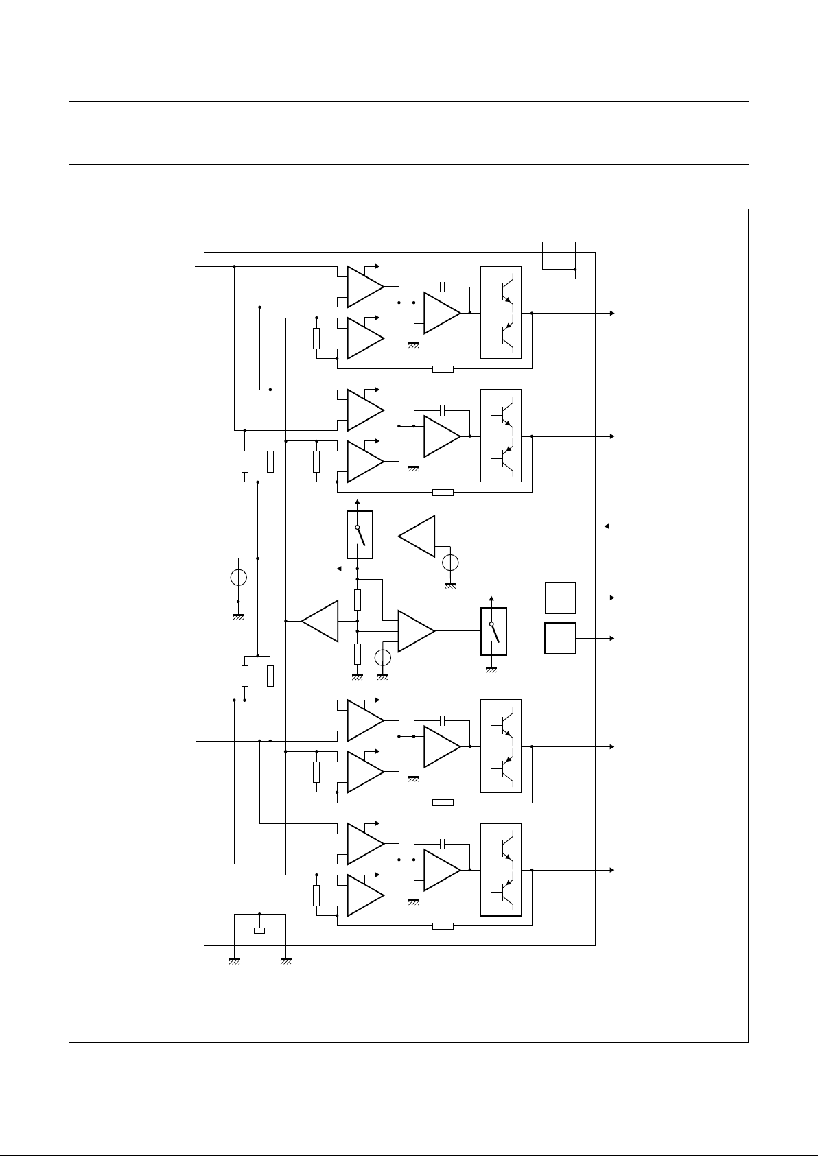
BLOCK DIAGRAM
handbook, full pagewidth
+
−
+
−
C
M
V
A
(9×)
2.3 kΩ
2.3
kΩ
mute
switch
+
−
+
−
C
M
V
A
V
A
1×
standby
reference
voltage
standby
switch
mute
reference
voltage
V
ref
mute
switch
CLIP
(9×)
2.3 kΩ
2.3
kΩ
60
kΩ
60
kΩ
60
kΩ
60
kΩ
mute
switch
+
−
+
−
C
M
V
A
(9×)
2.3 kΩ
2.3
kΩ
mute
switch
+
−
+
−
C
M
V
A
11 7
12
10
15
4
TDA8566Q
14
8
6
135
1
2
3
16
17
V
P2
V
P1
PGND2 PGND1
OUT2−
OUT2+
OUT1−
OUT1+
IN1−
IN1+
IN2−
IN2+
SGND
n.c.
DIAG
MODE
CLIP
MGD105
(9×)
2.3 kΩ
2.3
kΩ
mute
switch
9
DIAG
Fig.1 Block diagram.
2000 Jan 28 4
Philips Semiconductors Product specification
2 × 40 W/2 Ω stereo BTL car radio power amplifier
with differential inputs and diagnostic outputs
TDA8566Q
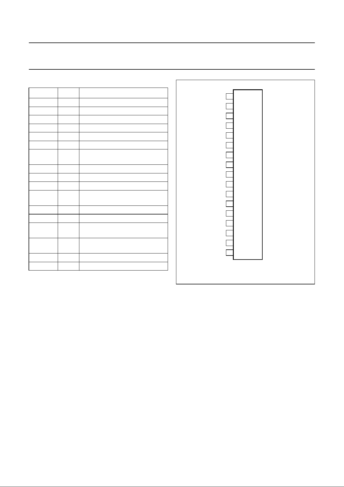
PINNING
SYMBOL PIN DESCRIPTION
IN1+ 1 channel 1 input positive
IN1− 2 channel 1 input negative
SGND 3 small signal ground
CLIP 4 clip detection
V
P1
5 supply voltage 1
OUT1+ 6 channel 1 speaker output positive
PGND1 7 channel 1 negative power supply
(ground)
OUT1− 8 channel 1 speaker output negative
n.c. 9 not connected
OUT2+ 10 channel 2 speaker output positive
PGND2 11 channel 2 negative power supply
(ground)
OUT2− 12 channel 2 speaker output negative
V
P2
13 supply voltage 2
MODE 14 mode select switch
(standby/mute/operating)
DIAG 15 short-circuit and temperature
pre-warning diagnostic
IN2+ 16 channel 2 input positive
IN2− 17 channel 2 input negative
handbook, halfpage
TDA8566Q
MGD101
1
2
3
4
5
6
7
8
9
10
11
12
13
14
15
16
17
IN1+
IN1−
SGND
CLIP
V
P1
OUT1+
PGND1
OUT1−
n.c.
IN2−
IN2+
DIAG
MODE
V
P2
OUT2−
PGND2
OUT2+
Fig.2 Pin configuration.
FUNCTIONAL DESCRIPTION
The TDA8566Qcontains 2 identical amplifiersandcan be
used for BTL applications. The gain of each amplifier is
fixed at 26 dB. Special features of this device are:
1. Mode select switch
2. Clip detection
3. Short-circuit diagnostic
4. Temperature pre-warning
5. Open-collector outputs
6. Differential inputs.
Mode select switch (pin 14)
• Standby: low supply current (<100 µA)
• Mute: input signal suppressed
• Operating: normal on condition.
Since this pinhasa very low input current (<40 µA),a low
cost supply switch can be applied. To avoid switch-on
plops,it isadvisable tokeepthe amplifierin themutemode
for a period of ≥150 ms (charging the input capacitors at
pins 1, 2, 16 and 17). This can be realized by
microcontroller controlor by anexternal timing circuit (see
Fig.7).
Clip detection (pin 4)
When clipping occurs at one or more output stages, the
dynamic distortion detector becomes active and pin 4
goes LOW. Thisinformation can be used to drivea sound
processor or a DC volume control to attenuate the input
signal and so limit the level of distortion. The output level
of pin 4 isindependent of the numberof channels that are
being clipped. The clip detection circuit is disabled in a
short-circuit condition, so if a fault condition occurs at the
outputs, pin 4 will remain at a HIGH level. The clip
detection waveforms are illustrated in Fig.3.
 Loading...