

Philips tda8561q DATASHEETS

INTEGRATED CIRCUITS
DATA SH EET
TDA8561Q
2 x 24 W BTL or 4 x 12 W
single-ended car radio power
amplifier
Preliminary specification
File under Integrated Circuits, IC01
July 1994

Philips Semiconductors Preliminary specification
2 x 24 W BTL or 4 x 12 W single-ended
TDA8561Q
car radio power amplifier
FEATURES
• Requires very few external components
• High output power
• Flexibility in use - Quad single-ended or stereo BTL
• Low output offset voltage
• Fixed gain
• Diagnostic facility (distortion, short-circuit and
temperature detection)
• Good ripple rejection
• Mode select switch (operating, mute and stand-by)
• Load dump protection
• AC and DC short-circuit safe to ground and to V
P
• Low power dissipation in any short-circuit condition
• Thermally protected
QUICK REFERENCE DATA
SYMBOL PARAMETER CONDITIONS MIN. TYP. MAX. UNIT
V
P
I
ORM
I
P
I
sb
positive operating supply voltage 6 14.4 18 V
repetitive peak output current −−4A
total quiescent current − 80 − mA
stand-by current − 0.1 100 µA
Stereo BTL application
P
O
output power 4 Ω; THD = 10% − 24 − W
RR supply voltage ripple rejection 48 −−dB
V
no
input impedance 25 −−kΩ
Z
I
| DC output offset voltage −−150 mV
∆V
O
noise output voltage Rs= 0 Ω−70 −µV
Quad single-ended application
P
O
output power THD = 10%
4 Ω−7−W
2 Ω−12 − W
RR supply voltage ripple rejection 48 −−dB
V
no
input impedance 50 −−kΩ
Z
I
noise output voltage Rs= 0 Ω−50 −µV
• Reverse polarity safe
• Electrostatic discharge protection
• No switch-on/switch-off plop
• Flexible leads
• Low thermal resistance
• Identical inputs (inverting and non-inverting).
GENERAL DESCRIPTION
The TDA8561Q is an integrated class-B output amplifier in
a 17-lead single-in-line (SIL) power package. It contains 4
x 12 W single-ended or 2 x 24 W bridge amplifiers.
The device is primarily developed for car radio
applications.
July 1994 2

Philips Semiconductors Preliminary specification
2 x 24 W BTL or 4 x 12 W single-ended car
TDA8561Q
radio power amplifier
ORDERING INFORMATION
PACKAGE
EXTENDED TYPE NUMBER
PINS PIN POSITION MATERIAL CODE
TDA8561Q 17 DBS plastic SOT243R
Note
1. SOT243-1; 1996 August 30.
(1)
July 1994 3
Philips Semiconductors Preliminary specification
2 x 24 W BTL or 4 x 12 W single-ended car
radio power amplifier
non-inverting
input 1
inverting
input 2
supply voltage
ripple rejection
non-inverting
input 4
1
60
kΩ
2
kΩ
60
kΩ
3
2
kΩ
x1
4
17
60
kΩ
2
kΩ
18 kΩ
18 kΩ
stand-by
switch
VA
15 kΩ
15 kΩ
mute switch
VA
mute switch
VA
V
P
mute switch
VA
C
m
C
m
PROTECTIONS
thermal
short-circuit
mute
reference
voltage
C
m
power stage
power stage
stand-by
reference
voltage
mute
switch
V
P1
5
13
TDA8561Q
TDA8561Q
V
P2
6
output 1
8
output 2
mode
14
select
switch
16
diagnostic
output
12
output 4
July 1994 4
inverting
input 3
18 kΩ
mute switch
60
kΩ
15
2
kΩ
input
reference
voltage
2711
ground
(signal)
VA
18 kΩ
9
not connected
C
m
GND1 GND2
power stage
power stage
MEA858 - 1
power ground (substrate)
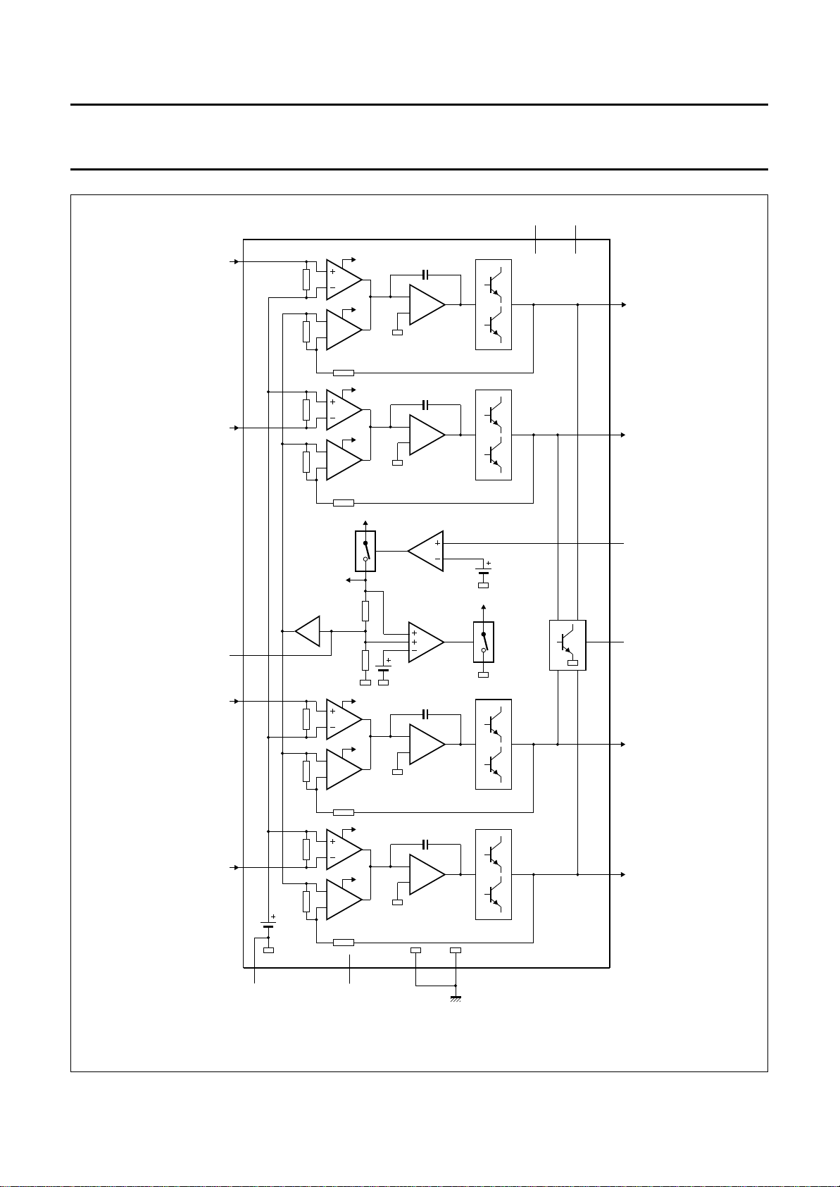
Fig.1 Block diagram.
10
output 3

Philips Semiconductors Preliminary specification
2 x 24 W BTL or 4 x 12 W single-ended car
radio power amplifier
PINNING
SYMBOL PIN DESCRIPTION
−INV 1 1 non-inverting input 1
GND(S) 2 signal ground
INV 2 3 inverting input 2
RR 4 supply voltage ripple rejection
V
P1
OUT 1 6 output 1
GND1 7 power ground 1
OUT 2 8 output 2
n.c. 9 not connected
OUT 3 10 output 3
GND2 11 power ground 2
OUT 4 12 output 4
V
P2
MODE 14 mode select switch input
INV 3 15 inverting input 3
V
DIAG
−INV 4 17 non-inverting input 4
FUNCTIONAL DESCRIPTION
The TDA8561Q contains four identical amplifiers and can
be used for single-ended or bridge applications. The gain
of each amplifier is fixed at 20 dB (26 dB in BTL).
Special features of the device are:
5 supply voltage
13 supply voltage
16 diagnostic output
INV 1
GND(S)
INV 2
RR
V
P1
OUT 1
GND1
OUTP 2
n.c.
OUT 3
GND2
OUTP 4
V
P2
MODE
INV 3
V
DIAG
INV 4
1
2
3
4
5
6
7
8
9
10
11
12
13
14
15
16
17
TDA8561Q
TDA8561Q
MEA859 - 1
Mode select switch (pin 14)
• low stand-by current (< 100 µA)
• low switching current (low cost supply switch)
• mute facility
To avoid switch-on plops, it is advised to keep the amplifier
in the mute mode during ≥ 100 ms (charging of the input
capacitors at pin 1, 3, 15 and pin 17).
This can be achieved by:
• microprocessor control
• external timing circuit (see Fig.11)
July 1994 5
Fig.2 Pin configuration.
Diagnostic output (pin 16)
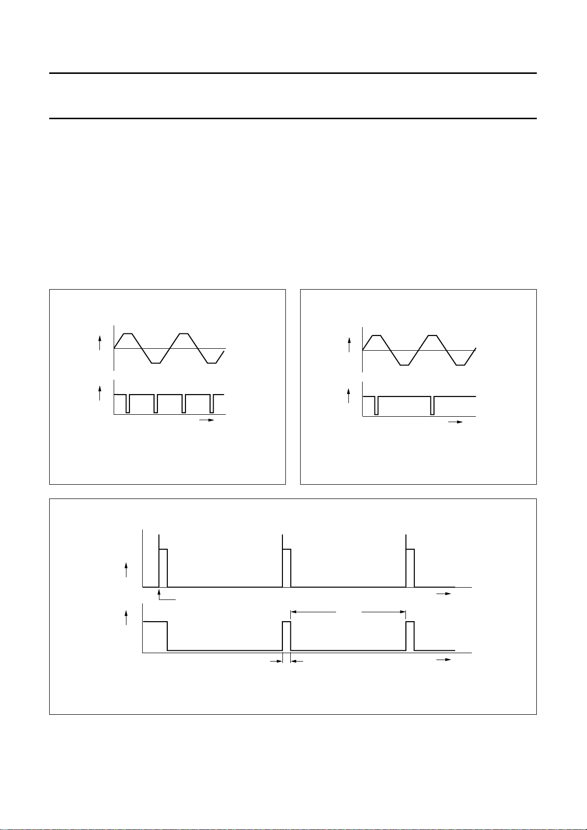
DYNAMIC DISTORTION DETECTOR (DDD)
At the onset of clipping of one or more output stages, the
dynamic distortion detector becomes active and pin 16
goes low. This information can be used to drive a sound
processor or DC volume control to attenuate the input
signal and thus limit the distortion. The output level of pin
16 is independent of the number of channels that are
clipping (see Fig.3 and Fig.4).
Philips Semiconductors Preliminary specification
2 x 24 W BTL or 4 x 12 W single-ended car
TDA8561Q
radio power amplifier
SHORT-CIRCUIT PROTECTION
When a short-circuit occurs at one or more outputs to ground or to the supply voltage, the output stages are switched off
until the short-circuit is removed and the device is switched on again, with a delay of approximately 20 ms, after removal
of the short-circuit. During this short-circuit condition, pin 16 is continuously low.
When a short-circuit across the load of one or both channels occurs the output stages are switched off during
approximately 20 ms. After that time it is checked during approximately 50 µs to see whether the short-circuit is still
present. Due to this duty cycle of 50 µs/20 ms the average current consumption during this short-circuit condition is very
low (approximately 40 mA).
During this short-circuit condition, pin 16 is low for 20 ms and high for 50 µs (see Fig.5).
The power dissipation in any short-circuit condition is very low.
ndbook, halfpage
V
O
0
MGA705
dbook, halfpage
V
O
0
MGA706
V
16
V
P
0
Fig.3 Distortion detector waveform; BTL
application.
handbook, full pagewidth
current
in
output
stage
V
15
short-circuit over the load
V
P
V
16
V
P
t
0
t
Fig.4 Distortion detector waveform; single-ended
application.
MGA707
t
20 ms
50 µs
t
July 1994 6
Fig.5 Short-circuit waveform.

Philips Semiconductors Preliminary specification
2 x 24 W BTL or 4 x 12 W single-ended car
TDA8561Q
radio power amplifier
TEMPERATURE DETECTION
When the virtual junction temperature Tvjreaches 150 °C, pin 16 will be active LOW.
OPEN COLLECTOR OUTPUT
Pin 16 is an open collector output, which allows pin 16 of more devices being tied together.
LIMITING VALUES
In accordance with the absolute maximum system (IEC 134).
SYMBOL PARAMETER CONDITIONS MIN. MAX. UNIT
v
p
I
OSM
I
ORM
T
stg
T
amb
T
vj
V
psc
V
pr
P
tot
positive supply voltage
operating − 18 V
non-operating − 30 V
load dump protection during 50 ms; t
≥ 2.5 ms − 45 V
r
non-repetitive peak output current − 6A
repetitive peak output current − 4A
storage temperature −55 +150 °C
operating ambient temperature −40 +85 °C
virtual junction temperature − 150 °C
AC and DC short-circuit safe voltage − 18 V
reverse polarity − 6V
total power dissipation − 60 W
THERMAL RESISTANCE
In accordance with IEC 747-1.
SYMBOL PARAMETER THERMAL RESISTANCE
R
R
th j-a
th j-c
from junction to ambient in free air 40 K/W
from junction to case (see Fig.6 and Fig.7) 1.3 K/W
July 1994 7
 Loading...