

Philips TDA8559T-N1 Datasheet

DATA SH EET
Product specification
Supersedes data of 1996 Jan 02
File under Integrated Circuits, IC01
1997 Jun 27
INTEGRATED CIRCUITS
TDA8559
Low-voltage stereo headphone
amplifier
1997 Jun 27 2
Philips Semiconductors Product specification
Low-voltage stereo headphone amplifier TDA8559
FEA TURES
• Operating voltage from 1.9 to 30 V
• Very low quiescent current
• Low distortion
• Few external components
• Differential inputs
• Usable as a mono amplifier in Bridge-Tied Load (BTL) or
stereo Single-Ended (SE)
• Single-ended mode without loudspeaker capacitor
• Mute and standby mode
• Short-circuit proof to ground, to supply voltage (<10 V)
and across load
• No switch on or switch off clicks
• ESD protected on all pins.
APPLICATIONS
• Portable telephones
• Walk-mans
• Portable audio
• Mains fed equipment.
GENERAL DESCRIPTION
The TDA8559 is a stereo amplifier that operates over a
wide supply voltage range from 1.9 to 30 V and consumes
a very low quiescent current. This makes it suitable for
battery fed applications (2 × 1.5 V cells). Because of an
internal voltage buffer, this device can be used with or
without a capacitor connected in series with the load. It can
be applied as a headphone amplifier, but also as a mono
amplifier with a small speaker (25 Ω), or as a line driver in
mains applications.
QUICK REFERENCE DATA
ORDERING INFORMATION
SYMBOL PARAMETER CONDITIONS MIN. TYP. MAX. UNIT
Supplies
V
P
operating supply voltage 1.9 3 30 V
I
q(tot)
total quiescent current − 2.75 4 mA
I
stb
standby supply current −−10 µA
Stereo application
P
o
output power THD = 10% 30 35 − mW
THD total harmonic distortion P
o
=20mW; fi= 1 kHz − 0.075 0.15 %
P
o
=20mW; fi= 10 kHz − 0.1 − %
G
v
voltage gain 25 26 27 dB
f
ss
small signal roll-off frequency −1dB − 750 − kHz
BTL application
P
o
output power THD = 10% 125 140 − mW
THD total harmonic distortion P
o
=70mW; fi= 1 kHz − 0.05 0.1 %
P
o
=70mW; fi= 10 kHz − 0.2 − %
G
v
voltage gain 31 32 33 dB
TYPE
NUMBER
PACKAGE
NAME DESCRIPTION VERSION
TDA8559 DIP16 plastic dual in-line package; 16 leads (300 mil); long body SOT38-1
TDA8559T SO16 plastic small outline package; 16 leads; body width 3.9 mm SOT109-1
1997 Jun 27 3
Philips Semiconductors Product specification
Low-voltage stereo headphone amplifier TDA8559
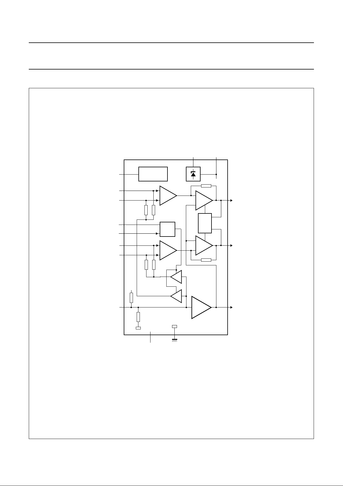
BLOCK DIAGRAM
Fig.1 Block diagram.
handbook, full pagewidth
+
−
+
−
+
−
+
−
OA
INPUT
LOGIC
V/I
REFERENCE
V/I
1
STANDBY
+IN1
−IN1
+IN2
−IN2
MUTE
MODE
SVRR
n.c. GND
2
3
5
6
4
12
BUFFER
OUT2
OUT1
MGD115
11
14
1615
139,10
7
8
V
P
V
P
V
P1
V
P2
BUFFER
OA
50 kΩ
100 kΩ
100
kΩ
50 kΩ
50 kΩ
50 kΩ
50
kΩ
50
kΩ
TDA8559
DQC

1997 Jun 27 4
Philips Semiconductors Product specification
Low-voltage stereo headphone amplifier TDA8559
PINNING
SYMBOL PIN DESCRIPTION
STANDBY 1 standby select
+IN1 2 non-inverting input 1
−IN1 3 inverting input 1
SVRR 4 supply voltage ripple rejection
+IN2 5 non-inverting input 2
−IN2 6 inverting input 2
MUTE 7 mute select
MODE 8 input mode select
n.c. 9 not connected
n.c. 10 not connected
OUT2 11 output 2
BUFFER 12 buffer output (0.5V
P
)
GND 13 ground
OUT1 14 output 1
V
P2
15 high supply voltage
V
P1
16 low supply voltage
Fig.2 Pin configuration.
handbook, halfpage
TDA8559
MGD114
1
2
3
4
5
6
7
8
STANDBY
+IN1
−IN1
SVRR
+IN2
−IN2
MUTE
MODE
V
P2
V
P1
OUT1
GND
BUFFER
OUT2
n.c.
n.c.
16
15
14
13
12
11
10
9
FUNCTIONAL DESCRIPTION
The TDA8559 contains two amplifiers with differential
inputs, a 0.5VP output buffer and a high supply voltage
stabilizer. Each amplifier consists of a voltage-to-current
converter (V/I), an output amplifier and a common dynamic
quiescent current controller. The gain of each amplifier is
internally fixed at 26 dB (= 20 ×). The 0.5VP output can be
used as a replacement for the single-ended capacitors.
The two amplifiers can also be used as a mono amplifier in
a BTL configuration thereby resulting in more output
power.
With three mode select pins, the device can be switched
into the following modes:
1. Standby mode (I
P
<10µA)
2. Mute mode
3. Operation mode, with two input selections (the input
source is directly connected or connected via coupling
capacitors at the input).
The ripple rejection in the stereo application with a
single-ended capacitor can be improved by connecting a
capacitor between the 0.5VP capacitor pin and ground.
The device is fully protected against short-circuiting of the
output pins to ground, to the low supply voltage pin and
across the load.
V/I converters
The V/I converters have a transconductance of 400 µS.
The inputs are completely symmetrical and the two
amplifiers can be used in opposite phase. The mute mode
causes the V/I converters to block the input signal.
The input mode pin selects two applications in which the
V/I converters can be used.
The first application (input mode pin floating) is used with
a supply voltage below 6 V. The input DC level is at ground
level (the unused input pin connected to ground) and no
input coupling capacitors are necessary. The maximum
converter output current is sufficient to obtain an output
swing of 3 V (peak).
In the second application with a supply voltage greater
than 6 V (input mode pin HIGH), the input mode pin is
connected to VP. In this configuration (input DC
level = 0.5VP+ 0.6 V) the input source must be coupled
with a capacitor and the two unused input pins must be
connected via a capacitor to ground, to improve noise
performance. This application has a higher quiescent
current, because the maximum output current of the V/I
converter is higher to obtain an output voltage swing of
9 V (peak).

1997 Jun 27 5
Philips Semiconductors Product specification
Low-voltage stereo headphone amplifier TDA8559
Output amplifiers
The output amplifiers have a transresistance of 50 kΩ, a
bandwidth of approximately 750 kHz and a maximum
output current of 100 mA. The mid-tap output voltage
equals the voltage applied at the non-inverting pin of the
output amplifier. This pin is connected to the output of the
0.5VP buffer. This reduces the distortion when the load is
connected between an output amplifier and the buffer
(because feedback is applied over the load).
Buffer
The buffer delivers 0.5V
P
to the output with a maximum
output (sink and source) current of 200 mA (peak).
Dynamic quiescent controller
The Dynamic Quiescent Current controller (DQC) gives
the advantage of low quiescent current and low distortion.
When there are high frequencies in the output signal, the
DQC will increase the quiescent current of the two output
amplifiers and the buffer. This will reduce the cross-over
distortion that normally occurs at high frequencies and low
quiescent current. The DQC gives output currents that are
linear with the amplitude and the frequency of the output
signals. These currents control the quiescent current.
Stabilizer
The TDA8559 has a voltage supply range from
1.9 to 30 V. This range is divided over two supply voltage
pins. Pin 16 is 1.9 to 18 V (breakdown voltage of the
process); this pin is preferred for supply voltages less than
18 V. Pin 15 is used for applications where V
P
is
approximately 6 to 30 V. The stabilizer output is internally
connected to the supply voltage pin 16. In the range from
6 to 18 V, the voltage drop to pin 16 is 1 V. In the range
from 18 to 30 V the stabilizer output voltage (to pin 16) is
approximately 17 V.
Input logic
The MUTE pin (pin 7) selects the mute mode of the V/I
converters. LOW (TTL/CMOS) level is mute. A voltage
between 0.5 V (low level) and 1.5 V (high level) causes a
soft mute to operate (no plops). When pin 7 is floating or
greater than 1.5 V it is in the operating condition.
The input mode pin must be connected to V
P
when the
supply voltage is greater than 6 V. The input mode logic
raises the tail current of the V/I converters and enables the
two buffers to bias the inputs of the V/I converters.
Reference
This circuit supplies all currents needed in this device. With
the standby mode pin 1 (TTL/CMOS), it is possible to
switch to the standby mode and reduce the total quiescent
current to below 10 µA.
1997 Jun 27 6
Philips Semiconductors Product specification
Low-voltage stereo headphone amplifier TDA8559
LIMITING VALUES
In accordance with the Absolute Maximum Rating System (IEC 134).
QUALITY SPECIFICATION
Quality in accordance with
“SNW-FQ-611E
”, if this type is used as an audio amplifier. The number of the quality
specification can be found in the
“Quality Reference handbook”
. The handbook can be ordered using the code
9397 750 00192.
THERMAL CHARACTERISTICS
CHARACTERISTICS
V
P
=3V; T
amb
=25°C; fi= 1 kHz; unless otherwise specified.
SYMBOL PARAMETER CONDITIONS MIN. MAX. UNIT
V
P2(max)
maximum supply voltage (pin 15) − 30 V
V
P1(max)
maximum supply voltage (pin 16) − 18 V
V
i(max)
maximum input voltage − 18 V
I
ORM
peak output current repetitive − 150 mA
P
tot
total power dissipation SO16 − 1.19 W
DIP16 − 2.4 W
T
amb
operating ambient temperature −40 +85 °C
T
stg
storage temperature −55 +150 °C
T
vj
virtual junction temperature − 150 °C
t
sc
short-circuiting time VP<10V − 1 hour
SYMBOL DESCRIPTION VALUE UNIT
R
th j-a
thermal resistance from junction to ambient in free air
DIP16 52 K/W
SO16 105 K/W
SYMBOL PARAMETER CONDITIONS MIN. TYP. MAX. UNIT
DC characteristics
V
P
operating supply voltage note 1 1.9 3 30 V
I
q(tot)
total quiescent current open load − 2.75 4 mA
I
stb
standby supply current open load −−10 µA
V
1
standby mode voltage standby 0 − 0.5 V
operating 1.5 − 18 V
V
7
mute mode voltage mute 0 − 0.5 V
operating 1.5 − 18 V
I
bias
input bias current − 100 300 nA

1997 Jun 27 7
Philips Semiconductors Product specification
Low-voltage stereo headphone amplifier TDA8559
Notes
1. The supply voltage range at pin VP1 is from 1.9 to 18 V. Pin VP2 is used for the voltage range from 6 to 30 V.
2. Measured with low-pass filter 30 kHz.
3. Noise output voltage measured with a bandwidth of 20 Hz to 20 kHz, unweighted. Rs=5kΩ.
4. RMS output voltage in mute is measured with Vi= 200 mV (RMS); f = 1 kHz.
5. DC output offset voltage is measured between the signal output and the 0.5VP output.
6. The ripple rejection is measured with a ripple voltage of 200 mV (RMS) applied to the positive supply rail (Rs=0kΩ).
7. DC output offset voltage is measured between the two signal outputs.
Single-ended stereo application (R
L
=32Ω)
P
o
output power THD = 10% 30 35 − mW
THD total harmonic distortion P
o
=20mW; fi= 1 kHz; note 2 − 0.075 0.15 %
P
o
=20mW; fi= 10 kHz; note 2 − 0.1 − %
G
v
voltage gain 25 26 27 dB
f
ss
small signal roll-off frequency −1dB − 750 − kHz
α
cs
channel separation Rs=5kΩ 40 −−dB
∆G
v
channel unbalance −−1dB
V
no
noise output voltage note 3 − 70 85 µV
V
no(mute)
noise output voltage in mute note 3 − 20 30 µV
V
o(mute)
output voltage in mute note 4 −−30 µV
V
mt
mid-tap voltage 1.4 1.5 1.6 V
Z
i
input impedance 75 100 125 kΩ
V
os
DC output offset voltage note 5 −−100 mV
SVRR supply voltage ripple rejection note 6 45 55 − dB
BTL application (R
L
=25Ω)
P
o
output power THD = 10% 125 140 − mW
THD total harmonic distortion P
o
=70mW; fi= 1 kHz; note − 0.05 0.1 %
P
o
=70mW; fi= 10 kHz; note 2 − 0.1 − %
G
v
voltage gain 31 32 33 dB
f
ss
small signal roll-off frequency −1dB − 750 − kHz
V
no
noise output voltage note 3 − 100 120 µV
V
no(mute)
noise output voltage in mute note 3 − 25 40 µV
V
o(mute)
output voltage in mute note 4 −−40 µV
V
os
DC output offset voltage note 7 −−150 mv
SVRR supply voltage ripple rejection note 6 39 49 − dB
Z
i
input impedance 39 50 61 kΩ
Line driver application (R
L
≥ 1kΩ)
V
o
line output voltage 0.1 − 2.9 V
SYMBOL PARAMETER CONDITIONS MIN. TYP. MAX. UNIT

1997 Jun 27 8
Philips Semiconductors Product specification
Low-voltage stereo headphone amplifier TDA8559
APPLICATION INFORMATION
General
For applications with a maximum supply voltage of 6 V
(input mode LOW) the input pins need a DC path to ground
(see Figs 3 and 4). For applications with supply voltages in
the range from 6 to 18 V (input mode HIGH) the input DC
level is 0.5V
P
+ 0.6 V. In this situation the input
configurations illustrated in Figs 5 and 6 have to be used.
The capacitor Cb is recommended for stability
improvement. The value may vary between
10 and 100 nF. This capacitor should be placed close to
the IC between pin 12 and pin 13.
Heatsink design
The standard application is stereo headphone
single-ended with a 32 Ω load impedance to buffer
(see Fig.9). The headphone amplifier can deliver a peak
output current of 150 mA into the load.
For the DIP16 envelope R
th j-amb
= 52 K/W; the maximum
sine wave power dissipation for T
amb
=25°C is:
For T
amb
=60°C the maximum total power dissipation is:
For the SO16 envelope R
th j-amb
= 105 K/W; the maximum
sinewave power dissipation for T
amb
=25°C is:
For T
amb
=60°C the maximum total power dissipation is:
2.4 W
150 25–
52
----------------------
=
1.7 W
150 60–
52
----------------------
=
1.2 W
150 25–
105
----------------------
=
0.85 W
150 60–
105
----------------------
=
Test conditions
T
amb
=25°C; unless otherwise specified: VP=3V,
f = 1 kHz, RL=32Ω, Gain = 26 dB, low input mode,
band-pass filter: 22 Hz to 30 kHz. The total harmonic
distortion as a function of frequency was measured with
low-pass filter of 80 kHz. The quiescent current has been
measured without any load impedance.
In applications with coupling capacitors towards the load,
an electrolytic capacitor has to be connected to pin 4
(SVRR).
• The graphs for the single-ended application have been
measured with the application illustrated in Fig.9; input
configuration for input mode low (Fig.4) and input
configuration for input mode high (Fig.6).
• The graphs for the BTL application ‘input mode low’
have been measured with the application circuit
illustrated in Fig.11 and the input configuration
illustrated in Fig.4.
• The graphs for the line-driver application have been
measured with the application circuit illustrated in Fig.13
and the input configuration illustrated in Fig.6; input
mode high.
Input configurations
The IC can be applied in two ways, ‘input mode low’ and
‘input mode high’. This can be selected by the input mode
at pin 8:
1. Input mode low: pin 8 floating:
The DC level of the input pins has to be between 0 V
and (V
P
− 1.8 V). A DC path to ground is needed.
The maximum output voltage is approximately
2.1 V (RMS). Input configurations illustrated in
Figs 3 and 4 should be used.
2. Input mode high: pin 8 is connected to VP:
This mode is intended for supply voltages >6 V. It can
deliver a maximum output voltage of approximately
6 V (RMS) at THD = 0.5%. The DC voltage level of the
input pins is (0.5VP+ 0.6 V). Coupling capacitors are
necessary. Input configurations illustrated in
Figs 5 and 6 should be used.

1997 Jun 27 9
Philips Semiconductors Product specification
Low-voltage stereo headphone amplifier TDA8559
Fig.3 Input configuration; with input capacitor
(VP< 6 V).
2.2 µF
V
IN
MGD123
5 kΩ INPUT
pins 2 and 5
pins 3 and 6
Fig.4 Input configuration; without input capacitor
(VP< 6 V).
handbook, halfpage
V
IN
MGD124
INPUT
pins 2 and 5
pins 3 and 6
Fig.5 Input configuration (VP> 6 V).
220 nF
V
IN
MGD125
220 nF
INPUT
pins 2 and 5
pins 3 and 6
Fig.6 Input configuration (at VP> 6 V, combined
negative inputs).
220
nF
100 nF
100 nF
V
IN
V
IN
MGD126
pin 2
pin 3
pin 6
pin 5
Fig.7 Soft mute.
V
P
7
mute
620 kΩ
47 kΩ
220 nF
MGL135
Standby/mute
• The standby mode (V1< 0.5 V) is intended for power
saving purpose. Then the total quiescent current is
<10 µA.
• To avoid ‘pop-noise’ during switch-on or switch-off the
IC can be muted (V7< 0.5 V). This can be achieved by
a ‘soft-mute’ circuit or by direct control from a
microcontroller.

1997 Jun 27 10
Philips Semiconductors Product specification
Low-voltage stereo headphone amplifier TDA8559
Application 1: SE with loudspeaker capacitor
(see Fig.8)
The value of capacitor Cr influences the behaviour of the
Supply Voltage Ripple Rejection (SVRR) at low
frequencies; increasing the value of Cr increases the
performance of the SVRR.
Application 2: SE to buffer (without loudspeaker
capacitor) (see Fig.9)
This is the basic headphone application. The advantage of
this application with respect to application 1, is that it
needs only one external component (Cb) in the event of
stability problems.
Application 3: Improved SE to buffer (without
loudspeaker capacitor) (see Fig.10)
This application is an improved configuration of
application 2. The distinction between the two is
connecting the loads in opposite phase. This lowers the
average current through the SE buffer.
It should be noted that a headphone cannot be used
because the load requires floating terminals.
Application 4: Bridge tied load mono amplifier
(see Fig.11)
This configuration delivers four times the output power of
the SE application with the same supply and load
conditions. The capacitor Cr is not required.
Application 5: Line driver application 1.9 V < V
P
<6V
(see Fig.12)
The TDA8559 delivers a virtual rail-to-rail output voltage
and is also usable in a low voltage environment, as a line
driver. In this application the input needs a DC path to
ground, input configurations illustrated in Figs 3 and 4
should be used. The value of capacitor Cr influences the
behaviour of the SVRR at low frequencies; increasing the
value of Cr increases the performance of the SVRR.
Application 6: Line driver application 6 V < V
P
<18V
(see Fig.13)
The TDA8559T delivers a virtual rail-to-rail output voltage.
Because the input mode has to be high, the input
configurations illustrated in Figs 5 and 6 should be used.
This application can also be used for headphone
application, however, due to the limited output current and
the limited output power at the headphone, series resistors
have to be used between the output pins and the load.
The value of capacitor Cr influences the behaviour of the
SVRR at low frequencies; increasing the value of Cr
increases the performance of the SVRR.
Application 7: Line driver application 6V < V
P
<30V
(see Fig.14)
With the supply voltage connected to pin 15 it is possible
to use the head amplifier above the maximum of 18 V to
pin 16. The internal supply voltage will be reduced to a
maximum of approximately 17 V.
This will be convenient in applications where the supply
voltage is higher than 18 V, however an output voltage
swing that reaches the higher supply voltage is not
required. the input configurations illustrated in
Figs 5 and 6 should be used. This application can also be
used for headphone applications. However, due to the
limited output current, series resistors have to be used
between the output pins and the load.
 Loading...