

Philips TDA8551T-N1 Datasheet

DATA SH EET
Product specification
Supersedes data of 1997 May 07
File under Integrated Circuits, IC01
1998 Feb 23
INTEGRATED CIRCUITS
TDA8551
1 W BTL audio amplifier with digital
volume control

1998 Feb 23 2
Philips Semiconductors Product specification
1 W BTL audio amplifier with digital volume control TDA8551
FEATURES
• One pin digital volume control
• Volume setting with UP/DOWN pulses
• Flexibility in use
• Few external components
• Low saturation voltage of output stage
• standby mode controlled by CMOS compatible levels
• Low standby current
• No switch-on/switch-off plops
• High supply voltage ripple rejection
• Protected against electrostatic discharge
• Outputs short circuit safe to ground, V
P
and across the
load
• Thermally protected.
GENERAL DESCRIPTION
The TDA8551; TDA8551T is a one channel 1 W
Bridge-Tied Load (BTL) audio power amplifier capable of
delivering 1 W output power to an 8 Ω load at THD = 10%
using a 5 V power supply. The circuit contains a BTL
power amplifier, a digital volume control and standby/mute
logic. The TDA8551T comes in an 8 pin SO package and
the TDA8551 in a 8 pin DIP package.
APPLICATIONS
• Portable consumer products
• Personal computers
• Telephony.
QUICK REFERENCE DATA
ORDERING INFORMATION
SYMBOL PARAMETER CONDITIONS MIN. TYP. MAX. UNIT
V
P
supply voltage 2.7 5 5.5 V
I
q
quiescent current VP=5V − 610mA
I
stb
standby current −−10 µA
P
o
output power THD = 10%; RL=8Ω; VP= 5 V 1 1.4 − W
G
v
voltage gain −60 − +20 dB
n
vol
number of volume steps − 64 −
THD total harmonic distortion P
o
= 0.5 W − 0.15 − %
SVRR supply voltage ripple rejection 48 −−dB
TYPE
NUMBER
PACKAGE
NAME DESCRIPTION VERSION
TDA8551T SO8 plastic small outline package; 8leads; body width 3.9 mm SOT96-1
TDA8551 DIP8 plastic dual in-line package; 8 leads (300 mil) SOT97-1
1998 Feb 23 3
Philips Semiconductors Product specification
1 W BTL audio amplifier with digital volume control TDA8551
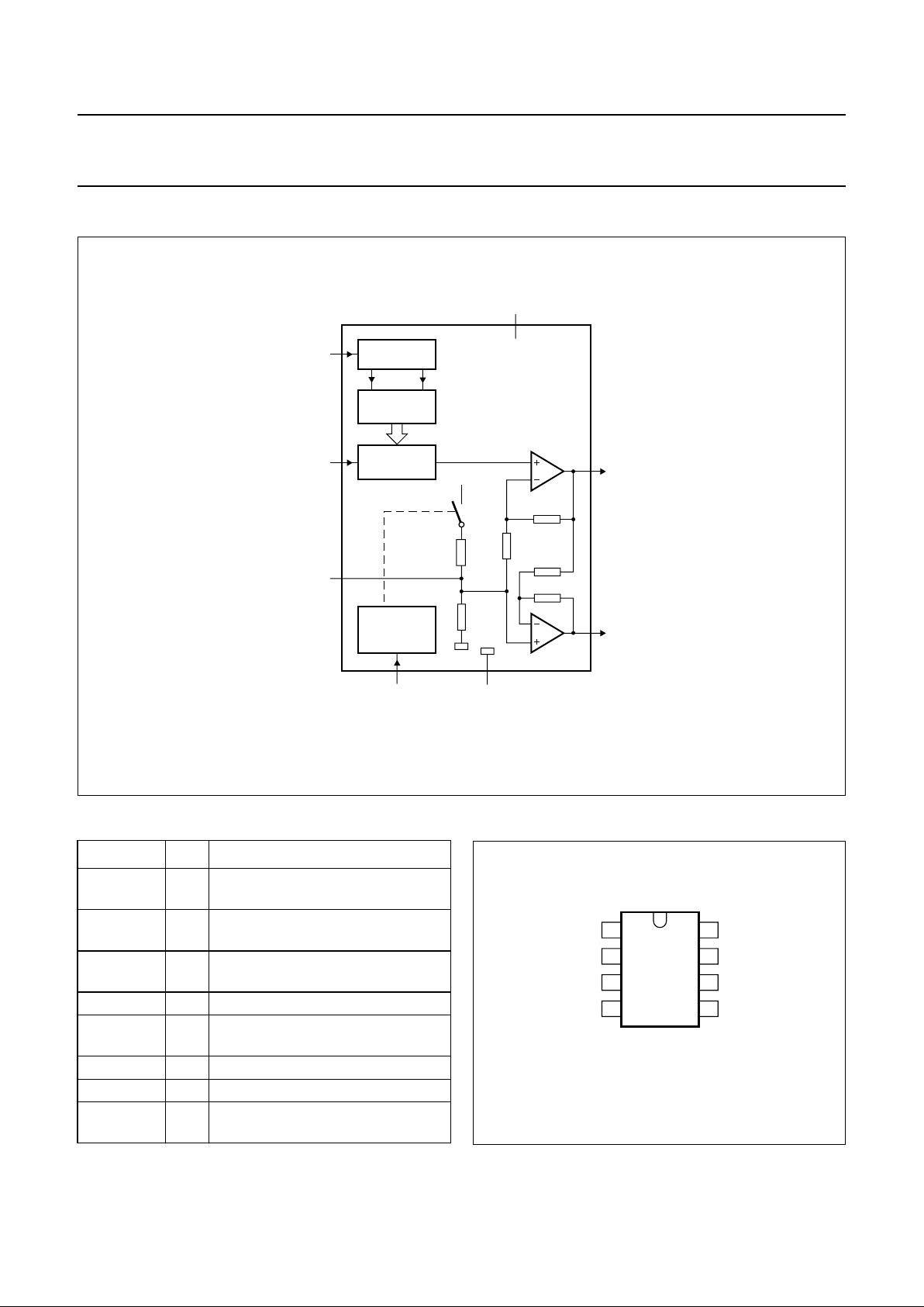
BLOCK DIAGRAM
Fig.1 Block diagram.
handbook, full pagewidth
MGK363
20 kΩ
TDA8551
5 kΩ
15 kΩ
15 kΩ
STANDBY/
MUTE/
OPERATING
VOLUME
CONTROL
UP/DOWN
COUNTER
INTERFACE
27
R
R
8
5
3
1
6
4
downup
V
P
V
P
SLAVE
MASTER
OUT+
GND
MODE
OUT−
IN
SVR
UP/DOWN
PINNING
SYMBOL PIN DESCRIPTION
UP/DOWN 1 digital trinary input for volume
control
MODE 2 digital trinary input for mode
selection (standby , mute, operating)
SVR 3 half supply voltage, decoupling
ripple rejection
IN 4 audio input
OUT− 5 negative loudspeaker output
terminal
V
P
6 supply voltage
GND 7 ground
OUT+ 8 positive loudspeaker output
terminal
Fig.2 Pin configuration.
handbook, halfpage
1
2
3
4
8
7
6
5
MGK362
TDA8551
OUT+
GNDMODE
V
P
OUT−
IN
SVR
UP/DOWN

1998 Feb 23 4
Philips Semiconductors Product specification
1 W BTL audio amplifier with digital volume control TDA8551
FUNCTIONAL DESCRIPTION
The TDA8551; TDA8551T is a 1 W BTL audio power
amplifier capable of delivering 1 W output power to an 8 Ω
load at THD = 10% using a 5 V power supply. The gain of
the amplifier can be set by the digital volume control. In the
maximum volume setting the gain is 20 dB. Using the
MODE pin the device can be switched to the standby
condition, the mute condition and the normal operating
condition. The device is protected by an internal thermal
shutdown protection mechanism.
Power amplifier
The power amplifier is a Bridge Tied Load (BTL) amplifier
with a complementary CMOS output stage. The total
voltage loss for both output power MOS transistors is
within 1 V and with a 5 V supply and an 8 Ω loudspeaker
an output power of 1 W can be delivered. The total gain of
this power amplifier is internally fixed at 20 dB.
Volume control
The volume control operates as a digital controlled
attenuator between the audio input pin and the power
amplifier. In the maximum volume control setting the
attenuation is 0 dB and in the minimum volume control
setting the typical attenuation is 80 dB. The attenuation
can be set in 64 steps by the UP/DOWN pin.
This UP/DOWN pin is a trinary input:
• Floating UP/DOWN pin: volume remains unchanged
• Negative pulses: setting volume towards minimum
• Positive pulses: setting volume towards maximum.
Each pulse on the UP/DOWN pin results in a change in
gain of 80/64 = 1.25 dB (typical value). In the basic
application the UP/DOWN pin is switched to ground or V
P
by a double push-button. When the supply voltage is
initially connected, after a complete removal of the supply,
the initial state of the volume control is an attenuation of
40 dB (low volume), so the gain of the total amplifier is
−20 dB. After powering-up, some positive pulses have to
be applied to the UP/DOWN pin for turning up to listening
volume. When the device is switched with the MODE
select pin to the mute or the standby condition, the volume
control attenuation setting remains on its value, assumed
that the voltage on pin VP does not fall below the minimum
supply voltage. After switching the device back to the
operation mode, the previous volume setting is
maintained.
Mode select pin
The device is in the standby mode (with a very low current
consumption) if the voltage at the MODE pin is between V
P
and VP− 0.5 V. At a mode select voltage level of less than
0.5 V the amplifier is fully operational. In the range
between 1 V and VP− 1.4 V the amplifier is in the mute
condition. The mute condition is useful for using it as a ‘fast
mute’; in this mode output signal is suppressed, while the
volume setting remains at its value. It is advised to keep
the device in the mute condition while the input capacitor
is being charged. This can be done by holding the MODE
pin at a level of 0.5VP, or by waiting approximately 100 ms
before giving the first volume-UP pulses.

1998 Feb 23 5
Philips Semiconductors Product specification
1 W BTL audio amplifier with digital volume control TDA8551
LIMITING VALUES
In accordance with the Absolute Maximum Rating System (IEC 134).
QUALITY SPECIFICATION
Quality according to
“SNW-FQ-611 part E”
, if this type is used as an audio amplifier. Quality specifications are listed in
the
“Quality reference handbook”
, order number 9397 750 00192.
THERMAL CHARACTERISTICS
SYMBOL PARAMETER CONDITIONS MIN. MAX. UNIT
V
P
supply voltage −0.3 +5.5 V
V
I
input voltage −0.3 VP+ 0.3 V
I
ORM
repetitive peak output current − 1A
T
stg
storage temperature −55 +150 °C
T
amb
operating temperature −40 +85 °C
V
sc
AC and DC short-circuit safe voltage − 5.5 V
P
tot
maximum power dissipation SO8 − 0.8 W
DIP8 − 1.2 W
SYMBOL PARAMETER CONDITIONS VALUE UNIT
R
th j-a
thermal resistance from junction to ambient in free air
SO8 160 K/W
DIP8 100 K/W

1998 Feb 23 6
Philips Semiconductors Product specification
1 W BTL audio amplifier with digital volume control TDA8551
CHARACTERISTICS
V
P
=5V; T
amb
=25°C; RL=8Ω; V
MODE
= 0 V; total gain setting at +7 dB (unless otherwise specified); measured in
test circuit of Fig.4.
SYMBOL PARAMETER CONDITIONS MIN. TYP. MAX. UNIT
DC characteristics
V
P
supply voltage 2.7 5 5.5 V
I
q
quiescent current RL= ∞; note 1 − 610 mA
I
stb
standby current V
MODE=VP
−−10 µA
V
O
DC output voltage note 2 − 2.5 − V
V
OUT+
− V
OUT−
differential output offset −−50 mV
Mode select pin
V
MODE
input voltage standby mode VP− 0.5 − V
P
V
mute mode 1 − V
P
− 1.4 V
operating mode 0 − 0.5 V
I
MODE
input current 0 < V
MODE<VP
−−100 nA
α mute attenuation note 3 80 90 − dB
Volume control
t
rep
pulse repetition time 100 −− ns
V
th(UP)
UP/DOWN pin up threshold level 4.2 − V
P
V
V
float(max)
UP/DOWN pin floating high level −−3.4 V
V
float(min
) UP/DOWN pin floating low level 1.0 −− V
V
th(DOWN)
UP/DOWN pin down threshold level 0 − 0.6 V
I
UP/DOWN
input current UP/DOWN pin 0 < V
UP/DOWN<VP
−−200 µA
G
v(max)
maximum voltage gain (including
power amplifier)
19 20 21 dB
G
v(min)
minimum voltage gain (including
power amplifier)
−62 −60 −58 dB
n
vol
number of volume steps − 64 −
∆G
v
voltage gain variation per step − 1.25 − dB
Z
i
input impedance 14 20 − kΩ
V
i(rms)(max)
maximum input voltage (RMS value) −−2.0 V
AC characteristics (f = 1 kHz)
P
o
output power THD = 10% 1 1.4 − W
THD = 0.5% 0.6 1.0 − W
THD total harmonic distortion P
o
= 0.5 W; note 4 − 0.15 0.5 %
V
n(o)
noise output voltage note 5 − 60 100 µV
SVRR supply voltage ripple rejection note 6 48 53 − dB
V
i(IN)(max)
maximum input voltage on pin IN THD = 1%;
Gv= −50 dB
to 0 dB
−−2.0 V
 Loading...