


DATA SH EET
Preliminary specification
Supersedes data of May 1993
File under Integrated Circuits, IC02
July 1994
INTEGRATED CIRCUITS
Philips Semiconductors
TDA8505
SECAM encoder

July 1994 2
Philips Semiconductors Preliminary specification
SECAM encoder TDA8505
FEATURES
• Two input stages, R, G, B and Y, −(R−Y), −(B−Y) with
multiplexing.
• Chrominance processing, highly integrated, includes
vertical identification, low frequency pre-emphasis and
high frequency pre-emphasis (anti-Cloche) and
bandpass filter.
• Fully controlled FM modulator which produces a signal
in accordance with the SECAM standard without
adjustments.
• Two reference oscillators, one for D'R f
0
(4.40625 MHz)
and one for D'B f0 (4.250 MHz). These oscillators are
tuned by PLL loop with the frequency of the line sync as
reference. Crystal tuning, or tuning by external
reference source, of the reference oscillators is
possible.
• Output stages, CVBS and separated Y + SYNC and
CHROMA. For CVBS output, signal amplitude 2 V (p−p)
nominal, thus only an external emitter follower is
required for 75 Ω driving.
• Sync separator circuit and pulse shaper, to generate the
required pulses for the processing, line, frame, FH/2 and
chrominance blanking.
• A 3-level sandcastle pulse is generated for PAL/NTSC
to SECAM transcoding.
• FH/2 input for locking with another decoder.
• Colour killing on the internal colour difference signals.
• Internal bandgap reference.
GENERAL DESCRIPTION
The TDA8505 is a highly integrated SECAM encoding IC
that is designed for use in all applications that require
transformation of R, G and B signals or Y, U and V signals
to a standard SECAM signal.
The specification of the input signals is fully compatible
with those of the TDA8501 PAL/NTSC encoder.
ORDERING INFORMATION
TYPE NUMBER
PACKAGE
PINS PIN POSITION MATERIAL CODE
TDA8505 32 SDIP32 plastic SOT232-1
July 1994 3
Philips Semiconductors Preliminary specification
SECAM encoder TDA8505
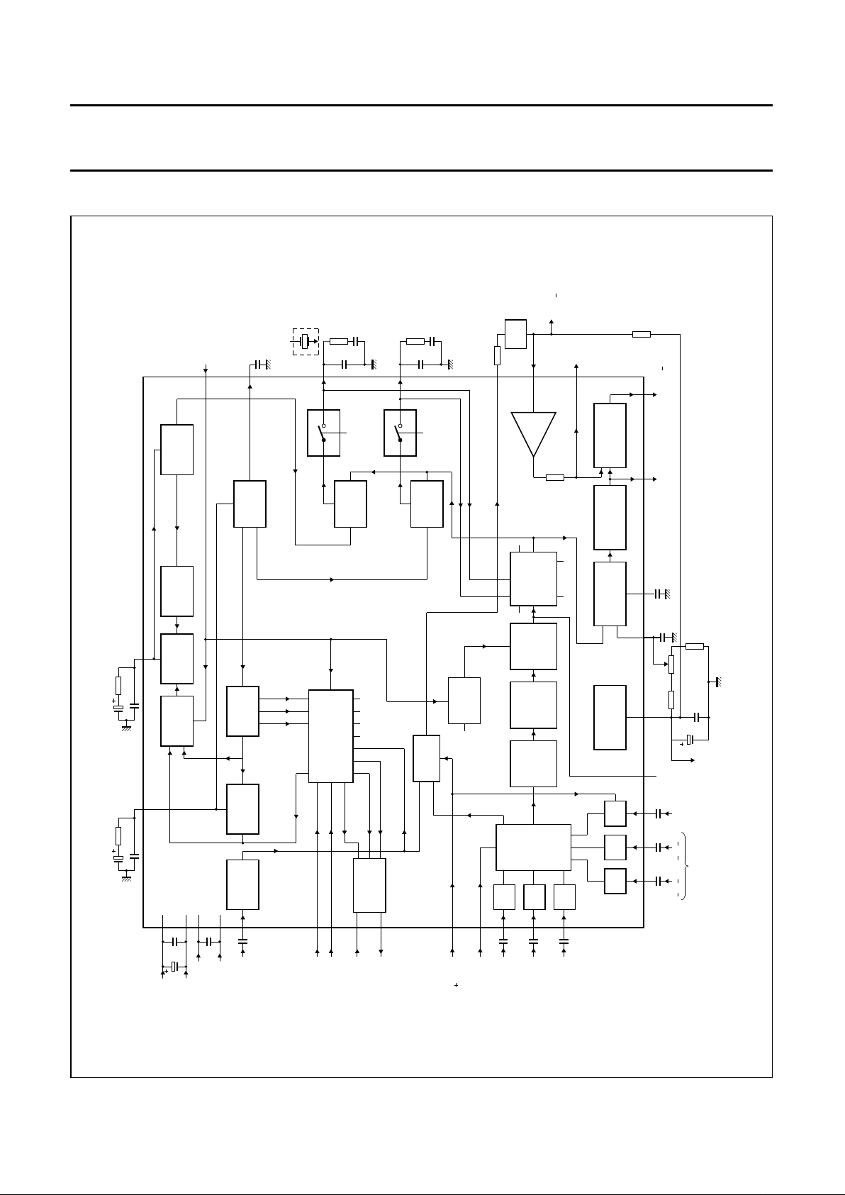
BLOCK DIAGRAM
handbook, full pagewidth
MLA951 - 3
PULSE
GENERATOR
PHASE
DETECTOR
272
DIVIDER
4.25 MHz
VCO
SYNC
SEPARATOR
SWITCH
PHASE
DETECTOR
282
DIVIDER
4.406 MHz
VCO
FRAME
IDENTI-
FICATION
CLAMP
ADDER
GAIN
LIMITER
FM
MODULATOR
PHASE
SWITCH
LOW-PASS
FILTER
LF PRE-
EMPHASIS
CHROMINANCE
BLANKING
RED
input
CL/BL
47
nF
7
GREEN
input
CL/BL
47
nF
9
BLUE
input
CL/BL
47
nF
11
MATRIX
SWITCH
SEQUENCE
CL/BL CL/BL CL/BL
1
47
nF
(R Y)
(B Y)
colour difference
inputs
luminance
input
3
47
nF
5
47
nF
multiplexer
control input
2
TEST
6
V
ref
V
ref
FADJ
14
reference
voltage
output
FLT output
FILTER
16
CLOCHE BANDPASS
ADDER
chrominance
output
18
21
CVBS 2 V (p p)
output
220
nF
BUFFER
2 kΩ
22
23
notch
output
Y+SYNC
1 V (p p)
DELAY
LINE
25
650
ns
PHASE
DETECTOR
LPFDB output
15
PHASE
DETECTOR
LPFDR output
13
ADDER
VCO4.25
output
control input
(Y/Y SYNC)
12
sandcastle
output
20
4
FH/2 input
28
colour killing
input
22 nF
composite
sync
input
29
30
32
10
8
V
SSD
V
DDD
V
SSA
V
DDA
47 µF
22
nF
100 nF
26
XTAL/PLL
VIDENT
input
LPF4.25
output
LPF 4.4
output
31
24
TDA8505
270 pF
27
Y+SYNC output
2 V (p-p)
Y+SYNC
input
17
19external power
supply (V )
ext
2.2 kΩ
4.7 µF
22 nF
1.2 kΩ
4.7 µF
100 nF
1 nF
3.9 kΩ
1 µF
6.8
nF
100 Ω
470 nF
SANDCASTLE
4.7
kΩ
1.8 kΩ
22 nF
22 kΩ
47
µF
22
nF
Fig.1 Block diagram.

July 1994 4
Philips Semiconductors Preliminary specification
SECAM encoder TDA8505
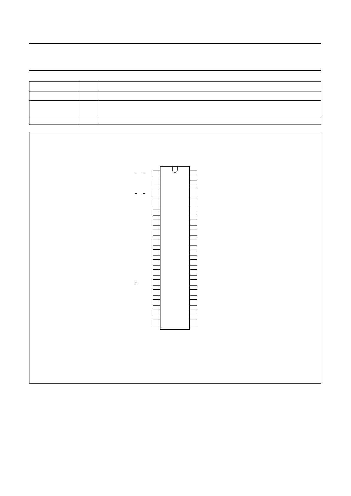
PINNING
D'R and D'B are the colour difference signals at the output of the multiplexer circuit; D'R = −1.9(R−Y) and
D'B = +1.5(B−Y), for an EBU bar of 75% the amplitudes are equal.
SYMBOL PIN DESCRIPTION
−(R−Y) 1 colour difference input signal, for EBU bar of 75% 1.05 V (peak-to-peak value)
MCONTR 2 multiplexer control; input HIGH = RGB, input LOW = −(R−Y), −(B−Y) and Y
−(B−Y) 3 colour difference input signal, for EBU bar of 75% 1.33 V (peak-to-peak value)
FH/2 4 line pulse input divided-by-2 for synchronizing two or more encoders; when not used this
pin is connected to ground
Y 5 luminance input signal 1 V nominal without sync
TEST 6 test pin; must be connected to V
CC
(pin 8), or left open-circuit
R 7 RED input signal for EBU bar of 75% 0.7 V (peak-to-peak value)
V
DDA
8 analog supply voltage for encoder part; 5 V nominal
G 9 GREEN input signal for EBU bar of 75% 0.7 V (peak-to-peak value)
V
SSA
10 analog ground
B 11 BLUE input signal for EBU bar of 75% 0.7 V (peak-to-peak value)
Y/Y+SYNC 12 when this control input is LOW, Y without sync is connected to pin 5, input blanking at
pin 5 is active; when input is HIGH, Y+SYNC is connected to pin 5, input blanking at pin 5
is not active
LPFDR 13 modulator control loop filter output; black level of D'R = 4.40625 MHz
FADJ 14 adjustment pin for 4.286 MHz of HF pre-emphasis filter
LPFDB 15 modulator control loop filter output; black level of D'B = 4.250 MHz
FLT 16 filter tuning loop capacitor output
V
ref
17 2.5 V internal reference voltage output
CHROMA 18 chrominance output, amplitude corresponds with Y+SYNC at the output of the delay line
V
ext
19 external power supply for sandcastle generation; when not used this pin is connected to
ground
SAND 20 3-level sandcastle output pulse
CVBS 21 composite SECAM output 2 V (peak-to-peak value) nominal
NOTCH 22 Y+SYNC output after an internal resistor of 2 kΩ; a notch filter can be connected
Y+SYNC IN 23 Y+SYNC input, connected to the output of the delay line
LPF4.4 24 loop filter output for 4.40625 MHz reference oscillator
Y+SYNC OUT 25 Y+SYNC output, 2 V (peak-to-peak value) nominal, connected to the input of the
delay line
XTAL/PLL
VIDENT
26 control pin; input HIGH = crystal tuning, input LOW = PLL tuning, both without vertical
identification, 2.5 V = PLL tuning with vertical identification
VCO4.25 27 when used for PLL tuning a capacitor is connected; when used for crystal tuning a crystal
has to be connected (in series with a capacitor)
COLKIL 28 colour killing; input HIGH = active, internal colour difference signals are blanked
CS 29 composite sync input, 0.3 V (peak-to-peak value) nominal
July 1994 5
Philips Semiconductors Preliminary specification
SECAM encoder TDA8505
V
SSD
30 digital ground
LPF4.25 31 loop filter output for 4.25 MHz reference oscillator; connected to pin 17 (V
ref
) when
external tuning by crystal or signal source
V
DDD
32 supply voltage for the digital part
SYMBOL PIN DESCRIPTION
handbook, halfpage
1
2
3
4
5
6
7
8
9
10
11
12
13
14
15
16
32
31
30
29
28
27
17
18
19
20
21
22
23
24
25
26
MLA952 - 3
MCONTR
FH/2
Y
TEST
R
V
DDA
G
V
DDD
LPF4.25
V
SSD
CS
COLKIL
VCO4.25
XTAL/PLL
VIDENT
LPF4.4
V
SSA
B
LPFDR
FADJ
LPFDB
FLT
V
ref
CHROMA
V
SAND
CVBS
NOTCH
Y/Y SYNC
(B Y)
Y+SYNC OUT
(R Y)
Y+SYNC IN
TDA8505
ext
Fig.2 Pin configuration.
July 1994 6
Philips Semiconductors Preliminary specification
SECAM encoder TDA8505
FUNCTIONAL DESCRIPTION
The following three important circuits are integrated:
• Encoder circuit
• Modulator control circuit
• Sync separator and pulse shaper.
Encoder circuit
I
NPUT STAGE
R, G and B inputs are connected to the matrix via a
clamping and a blanking circuit.
For an EBU colour bar of 75% the amplitude of the signal
must be 0.7 V (peak-to-peak value). The outputs of the
matrix are Y, D'R and D'B.
The second part of the input stage contains inputs for
colour difference signals and a luminance signal. The
condition for 75% colour bar is
−(R−Y) = 1.05 V (peak-to-peak value) at pin 1,
−(B−Y) = 1.33 V (peak-to-peak value) at pin 3 and
Y = 1 V (peak-to-peak value) without sync at pin 5. After
clamping and blanking the amplitude and polarity are
corrected such that the signals are equal to the signals of
the matrix output. Signals are connected to a switch. Fast
switching between the two input parts is possible by the
multiplexer control pin (pin 2).
The Y output signal of the multiplexer is added to the sync
pulse of the sync separator.
The Y input (pin 5) is different to the other 5 inputs. The
timing of the internal clamping is after the sync period and
there is no vertical blanking.
The input blanking of Y can be switched off by a HIGH at
pin 12, and the internal sync separator signal is not added
to the Y signal. In this way the Y+SYNC is allowed at pin 5
and after clamping internally connected directly to pin 25.
The colour difference signals are switched sequentially by
H/2 and fed to the low frequency pre-emphasis circuit.
The colour-killing input signal at pin 28 can be used for
completely blanking the internal colour difference signals
at the input of the low frequency pre-emphasis filter.
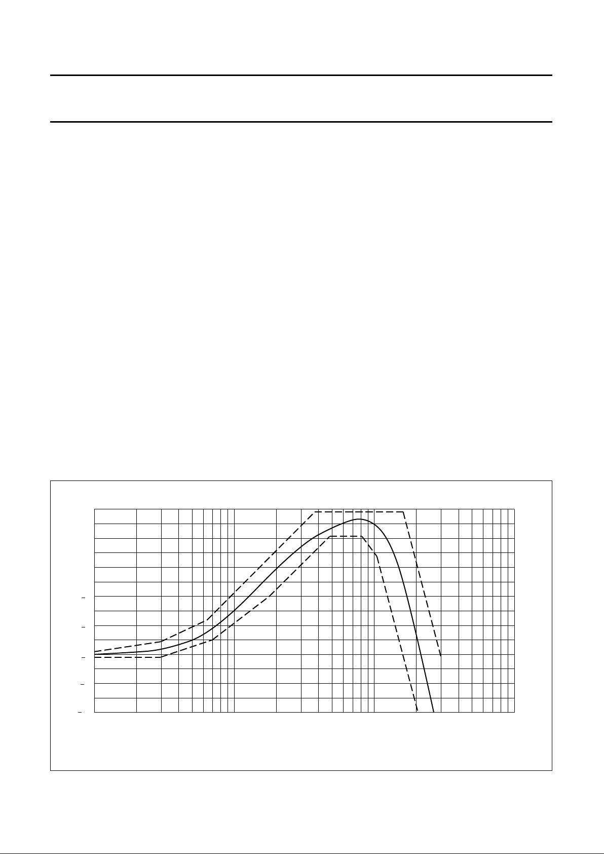
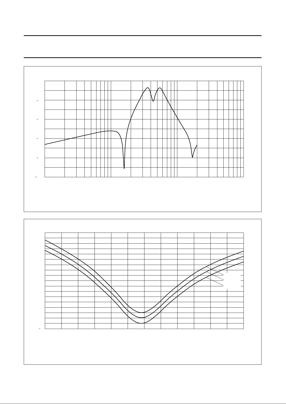
LOW FREQUENCY PRE-EMPHASIS
This filter is fully integrated, Fig.3 illustrates the nominal
response.
The transfer is guaranteed within the illustrated area for
the whole ambient temperature range by a compensation
circuit.
Fig.3 Nominal response for the low frequency pre-emphasis filter.
handbook, full pagewidth
10
MLA953 - 1
10
6
10
5
10
4
0
8
6
4
2
2
4
f (Hz)
H
(dB)
10
7
July 1994 7
Philips Semiconductors Preliminary specification
SECAM encoder TDA8505
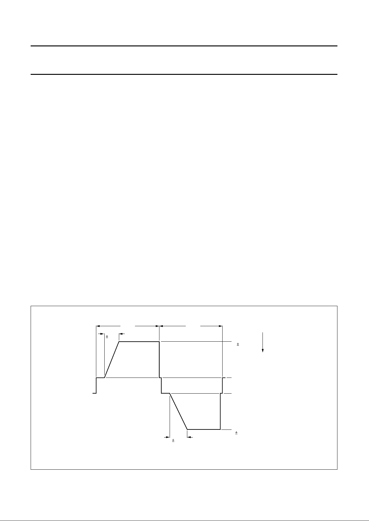
VERTICAL IDENTIFICATION
After the low frequency pre-emphasis the signal is
clamped and, if desired the vertical identification sawtooth
waveform can be added. The generation of the vertical
identification is switched on/off by the logic level input at
pin 26.
Figure 4 shows the sawtooth waveform at the input of the
FM modulator with the corresponding frequency values
after modulation.
Vertical identification is only possible if PLL tuning is
selected.
G
AIN + LIMITER
The gain of this amplifier is sequentially switched, so that
the amplitude of D'R is 280/230 times the amplitude of D'B
(based on an EBU colour bar). The signal is limited at a
lower and upper level to ensure that the FM modulator
frequencies are always between 3.9 MHz and 4.756 MHz.
A DC offset between D'R and D'B is added which
corresponds with the limiter levels.
FM
MODULATOR
The signal of the gain + limiter stage is fed to the FM
modulator.
The modulator control adjusts the DC level at pin 13 to set
the frequency of the FM signal to 4.406 MHz at the black
level of D'R. The modulator control also sets the DC level
at pin 15 to adjust the FM frequency to 4.250 MHz at the
black level of D'B.
At the start of every line the FM modulator is stopped and
is started again by a short duration pulse of the pulse
shaper. These stop/start pulses are operating such that
after two lines starting in the same phase, the start phase
of the third line is shifted 180 degrees. This sequence is
inverted during each vertical blanking.
The FM signal is fed to the internal HF pre-emphasis filter.
HF PRE-EMPHASIS AND BANDPASS FILTER
An HF pre-emphasis filter combined with a bandpass filter
is integrated.
Figures 5 and 6 illustrate the frequency response. Two
resistors in series with a potentiometer at pin 14 adjusts
the frequency to 4.286 MHz with a tolerance of ±20 kHz.
A tuning circuit integrated with an external capacitor
connected to pin 16 guarantees a stable frequency
response for the whole temperature range.
The output of the bandpass filter is connected directly to
the chrominance blanking circuit.
Fig.4 Vertical identification sawtooth waveform input.
handbook, full pagewidth
MLA954
64 µs64 µs
3.90 MHz
4.250 MHz
4.406 MHz
4.756 MHz
frequency
after
modulation
35 kHz
35 kHz
D'R
D'B
18 sµ
6 sµ
15 sµ
5 sµ
July 1994 8
Philips Semiconductors Preliminary specification
SECAM encoder TDA8505
handbook, full pagewidth
MLA955 - 1
10
8
10
7
10
6
10
5
20
60
40
f (Hz)
0
80
100
H
(dB)
Fig.5 Frequency response of the HF pre-emphasis and bandpass filter; H as a function of frequency (1).
Fig.6 Frequency response of the HF pre-emphasis and bandpass filter; H as a function of frequency (2).
handbook, full pagewidth
4.9
16
2
3.7 4.1 4.5
MLA956 - 1
10
4
3.9 4.3 4.7
0
2
6
8
12
14
f (MHz)
upper limit
nominal
lower limit
H
(dB)
July 1994 9
Philips Semiconductors Preliminary specification
SECAM encoder TDA8505
CHROMINANCE BLANKING
The chrominance signal is blanked by the internally
generated chrominance blanking pulse. The output of this
blanking stage is connected to the chrominance and
CVBS output circuits.
Y+SYNC, CVBS,
AND CHROMA OUTPUTS
The Y output signal of the matrix is added to the composite
sync signal of the sync separator. The output of this adder
at pin 25 is connected to the input of an external delay line
which is necessary for correct timing of the Y+SYNC signal
corresponding with the chrominance signal. The signal
amplitude at pin 25 is 2 V (peak-to-peak value) nominal,
so at the output of the delay line Y+SYNC is
1 V (peak-to-peak value).
The delay line has to be DC-coupled between
pins 25 and 23 to ensure the required DC level at
pin 23. The output resistor of the delay line has to be
connected to pin 17 where (V
ref
= 2.5 V).
The output of the delay line is connected to pin 23 which is
the input of a buffer operational amplifier. The output of the
buffer operational amplifier is connected to pin 22 and to
the CVBS adder stage via an internal resistor of 2 kΩ. An
external notch filter can be connected to pin 22. The CVBS
signal amplitude output at pin 21 is 2 V (peak-to-peak
value) nominal. An external emitter follower is used to
provide a 75 Ω output load.
The amplitude of the chrominance output signal which is
connected to pin 18 corresponds with the Y+SYNC signal
at the output of the delay line.
Modulator control circuit
The modulator control circuit has two tuning modes which
are controlled by the input at pin 26:
• Tuning by line frequency
• Tuning by crystal or external signal source.
T
UNING BY LINE FREQUENCY
Two reference voltage controlled oscillators (VCOs) are
integrated, the 4.4 MHz VCO with an internal capacitor
and the 4.25 MHz VCO with an external capacitor at
pin 27.
A PLL loop with divider circuits directly couples the
frequencies of the two VCOs with the line frequency of the
sync separator sync signal.
The loop filter for the 4.40625 MHz reference is at pin 24
and the loop filter for the 4.250 MHz reference is at pin 31.
The outputs of the 272 divider are also used for pulse
shaping.
Within the vertical blanking period, another two Phase
Locked Loops (PLLs) synchronizes the FM modulator
during two lines with the 4.406 MHz reference VCO and
during the following 2 lines with the 4.250 MHz reference
VCO. The loop filters are connected to pins 13 and 15
respectively.
It is necessary to use low-leakage capacitors for these
loop filters.
T
UNING BY CRYSTAL OR EXTERNAL SIGNAL SOURCE
When the frequency of the sync pulse at pin 29 is not
stable or is incorrect it is possible to tune the FM modulator
using an external 4.250 MHz crystal connected to pin 27.
The 4.25 MHz loop at pin 31 has to be connected to pin 17
(V
ref
). A stable line frequency reference is generated by
the 272 divider circuit which is used for the 4.406 MHz
reference loop.
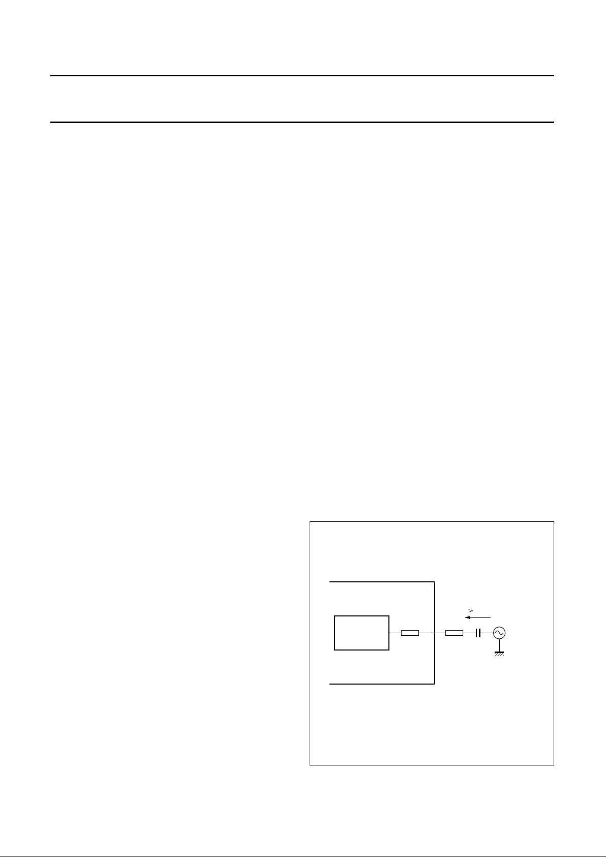
An external signal source, instead of a crystal, can be
connected at pin 27 via a capacitor in series with a resistor.
The minimum AC current of 50 µA is determined by the
resistor values (R
int+Rext
) and the output voltage of the
signal source (see Fig.7).
When crystal tuning is used no vertical identification
is possible.
Crystal tuning is recommended for VTR signals.
handbook, halfpage
MSA732 - 1
1 nF
R
ext
I 50 A
µ
signal
source
27
R
int
800Ω
OSCILLATOR
TDA8505
V (p-p)
Fig.7 Tuning circuit for external signal source.
July 1994 10
Philips Semiconductors Preliminary specification
SECAM encoder TDA8505
Sync separator and pulse shaper
The composite sync input at pin 29 together with the
outputs of the 272 divider of the 4.250 MHz reference loop
are the sources for all pulses necessary for the processing.
The pulses are used for:
• Clamping
• Video blanking
• FH/2
• Chrominance blanking
• Stop/start of modulator
• Vertical identification
• Timing for the modulator control
• Sandcastle pulse shaping at pin 20.
External FH/2 at pin 4 is only necessary when two or more
SECAM encoders have to be locked in the same phase.
The phase of the internal FH/2 can be locked with an
external FH/2 connected at pin 4. A reset of the internal
FH/2 is possible by forcing pin 4 to a HIGH level. This
HIGH level corresponds with D'R. Pin 4 is connected to
ground when not used.
Figures 9 and 10 show the generated pulses during
vertical blanking for PLL tuning or crystal tuning
respectively. Figure 11 shows the pulses during line
blanking.
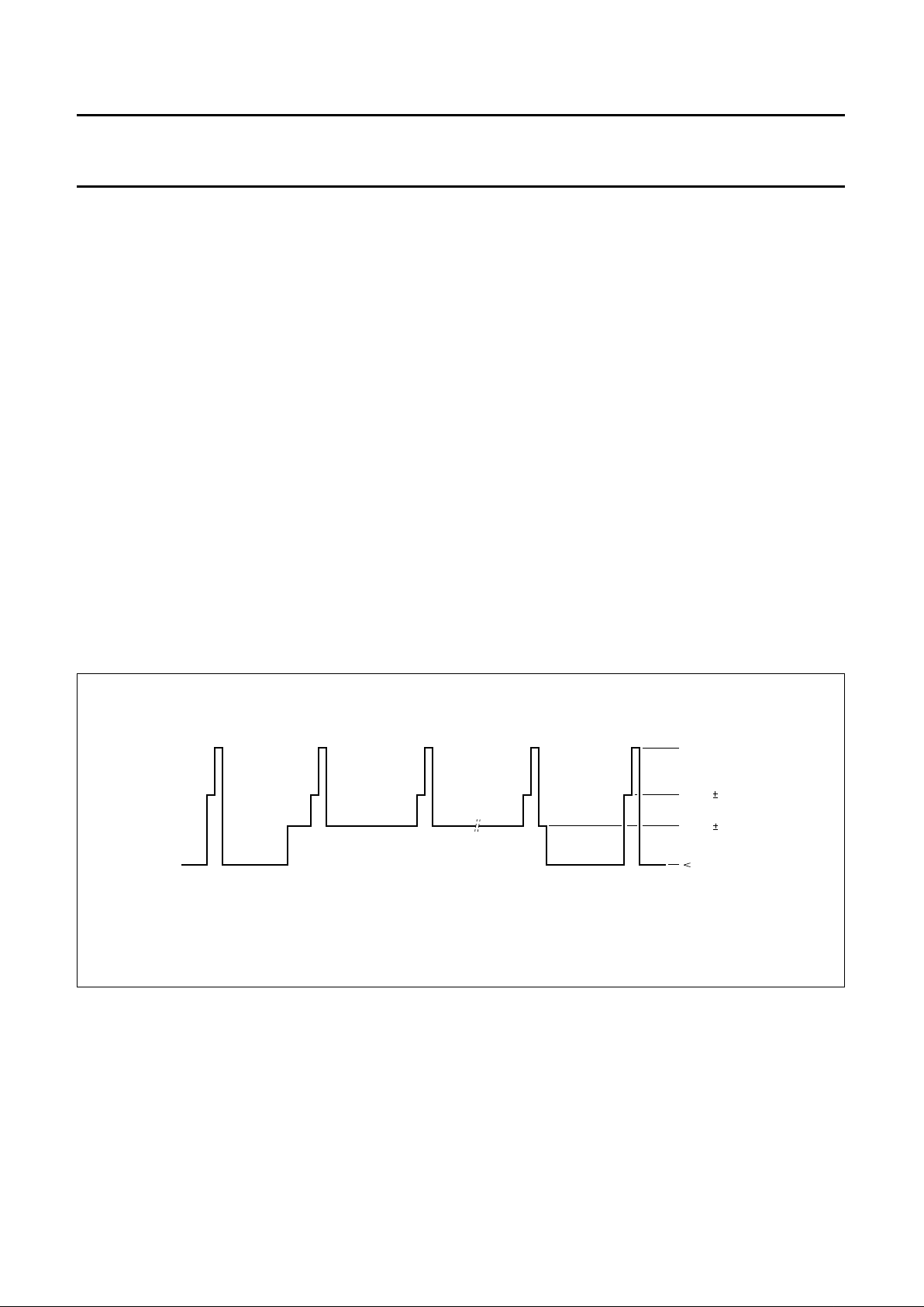
Transcoding application
A sandcastle pulse is necessary for the PAL/NTSC
demodulator (i.e. TDA4510) for transcoding PAL or NTSC
to SECAM.
Most of the demodulator ICs use a sandcastle pulse with
an amplitude of 12 V or 8 V. A 12 V or 8 V sandcastle is
not possible with the TDA8505 because of the 5 V power
supply.
To generate a 3-level sandcastle pulse at pin 20
(see Fig.8) an external supply voltage must be connected
to pin 19.
The PAL or NTSC CVBS signal is connected to the
composite sync input (pin 29) for PLL tuning and pulse
shaping. As previously mentioned the Y input at pin 5 can
be used as the Y+SYNC input for the filtered Y+SYNC PAL
or NTSC signal, when pin 12 is at a HIGH level.
Fig.8 3-level sandcastle pulse.
handbook, full pagewidth
MSA733 - 1
V
ext
4.5 V 0.2 V
2.5 V 0.2 V
0.5 V
 Loading...