

Philips TDA8362, TDA8361, TDA8360 Datasheet

INTEGRATED CIRCUITS
DATA SH EET
TDA8360; TDA8361; TDA8362
Integrated PAL and PAL/NTSC TV
processors
Objective specification
File under Integrated Circuits, IC02
Philips Semiconductors
March 1994

Philips Semiconductors Objective specification
Integrated PAL and PAL/NTSC TV
processors
FEATURES
Available in TDA8360, TDA8361
and TDA8362
• Vision IF amplifier with high
sensitivity and good differential
gain and phase
• Multistandard FM sound
demodulator (4.5 MHz to 6.5 MHz)
• Integrated chrominance trap and
bandpass filters (automatically
calibrated)
• Integrated luminance delay line
• RGB control circuit with linear RGB
inputs and fast blanking
• Horizontal synchronization with two
control loops and alignment-free
horizontal oscillator without
external components
• Vertical count-down circuit
(50/60 Hz) and vertical preamplifier
• Low dissipation (700 mW)
• Small amount of peripheral
components compared with
competition ICs
• Only one adjustment (vision IF
demodulator)
• The supply voltage for the ICs is
8 V. They are mounted in a shrink
DIL envelope with 52 pins and are
pin compatible.
Additional features
TDA8360
• Alignment-free PAL colour decoder
for all PAL standards, including
PAL-N and PAL-M.
TDA8361
• PAL/NTSC colour decoder with
automatic search system
• Source selection for external
audio/video (A/V) inputs (separate
Y/C signals can also be applied).
TDA8362
• Multistandard vision IF circuit
(positive and negative modulation)
• PAL/NTSC colour decoder with
automatic search system
• Source selection for external
A/V inputs (separate Y/C signals
can also be applied)
• Easy interfacing with the TDA8395
(SECAM decoder) for
multistandard applications.
TDA8360; TDA8361; TDA8362
GENERAL DESCRIPTION
The TDA8360, TDA8361 and
TDA8362 are single-chip TV
processors which contain nearly all
small signal functions that are
required for a colour television
receiver. For a complete receiver the
following circuits need to be added:
a base-band delay line (TDA4661),
a tuner and output stages for audio,
video and horizontal and vertical
deflection.
Because of the different functional
contents of the ICs the set maker can
make the optimum choice depending
on the requirements for the receiver.
The TDA8360 is intended for simple
PAL receivers (all PAL standards,
including PAL-N and PAL-M are
possible).
The TDA8361 contains a PAL/NTSC
decoder and has an A/V switch.
For real multistandard applications
the TDA8362 is available. In addition
to the extra functions which are
available in the TDA8361, the
TDA8362 can handle signals with
positive modulation and it supplies
the signals which are required for the
SECAM decoder TDA8395.
ORDERING INFORMATION
EXTENDED TYPE
NUMBER
TDA8360 52 shrink DIL plastic SOT247AG
TDA8361 52 shrink DIL plastic SOT247AG
TDA8362 52 shrink DIL plastic SOT247AG
March 1994 2
PINS PIN POSITION MATERIAL CODE
PACKAGE

Philips Semiconductors Objective specification
Integrated PAL and PAL/NTSC TV
TDA8360; TDA8361; TDA8362
processors
QUICK REFERENCE DATA
SYMBOL PARAMETER CONDITIONS MIN. TYP. MAX. UNIT
V
P
I
P
Input voltages
V
45,46(rms)
V
5(rms)
V
6(rms)
V
15(p-p)
V
22,23,24(p−p)
Output signals
V
O(p-p)
I
47
V
44
V
50(rms)
V
18,19,20(p-p)
I
37
I
43
Control voltages
V
control
supply voltage 7.2 8.0 8.8 V
supply current − 80 − mA
video IF amplifier sensitivity (RMS value) − 70 100 µV
sound IF amplifier sensitivity (RMS value) − 1 − mV
external audio input (RMS value) TDA8361, TDA8362 − 350 − mV
external CVBS input (peak-to-peak value) TDA8361, TDA8362 − 1 − V
RGB inputs (peak-to-peak value) − 0.7 − V
demodulated CVBS output
− 2.4 − V
(peak-to-peak value)
tuner AGC control current 0 − 5mA
AFC output voltage swing − 6 − V
audio output voltage (RMS value) − 700 − mV
RGB output signal amplitudes
− 4 − V
(peak-to-peak value)
horizontal output current 10 −−mA
vertical output current 1 −−mA
control voltages for Volume, Contrast,
0 − 5V
Saturation, Brightness, Hue and Peaking
March 1994 3
Philips Semiconductors Objective specification
Integrated PAL and PAL/NTSC TV
processors
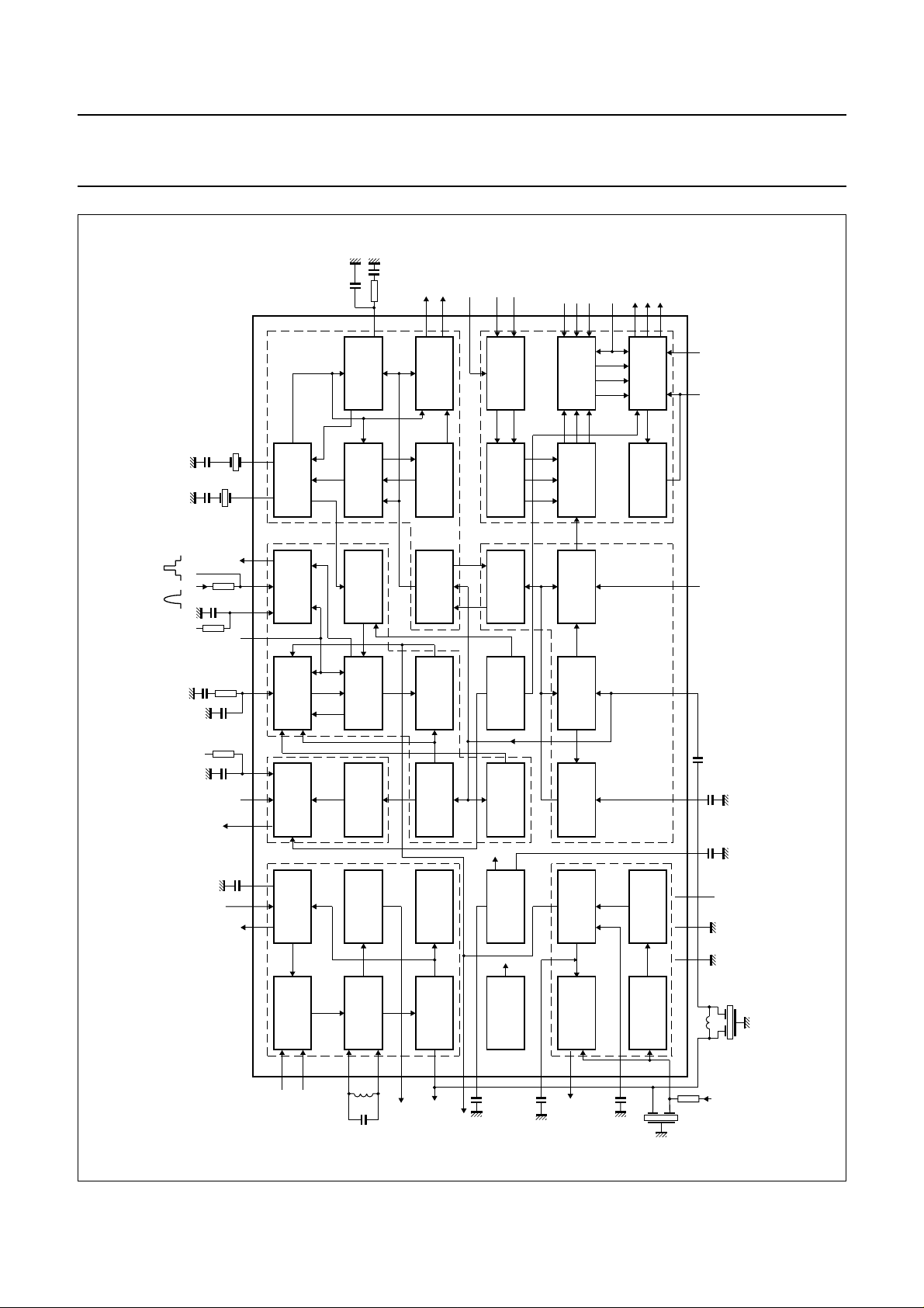
DET
33
PHASE
DETECTOR
FBI/SCO
flyback sandcastle
PH2LF
PH1LF
XTAL1 XTAL2
HOUT
VSTART
39 38 37 34 3543
36
XTAL
OSCILLATOR
PHASE 2
PHASE 1
KILLERS
COLOUR
TUNING
LINE
OSCILLATOR
to
TDA4661
R-Y output
B-Y output
30
31
DEMODULATOR
PAL
IDENTIFICATION
ACC
AMPLIFIER
DETECTOR
COINCIDENCE
SAT
26
TDA8360; TDA8361; TDA8362
from
TDA4661
B-Y input
R-Y input
28
29
SET
CLAMPS
MATRIX
BANDPASS
CHROMINANCE
RESET
POWER
RIN
222324
BIN
GIN
21
CLAMP
SWITCH
MATRIX
LUMINANCE
Y DELAY
PEAKING
BYPASS
TRAP AND
RGBIN
BOUT
GOUT
181920
OUTPUT
PWL
ROUT
STAGES
MLA621 - 1
17
13 14 25
BRIPEAKIN
CON
INT
CVBS
VRAMP
41 42 40
AGC
DEC
VOUT
ADJ
TUNE
VFB
AGCOUT
49
47 48
VERTICAL
AGC
IF
45
IFIN1
OUTPUT
AMPLIFIER
46
IFIN2
DIVIDER
VERTICAL
AFC AND
SAMPLE-
AND-HOLD
DEMODULATOR
2
3
IFDEM1
44
IFDEM2
AFCOUT
H AND V
SEPARATION
VIDEO
IDENTIFICATION
VIDEO
AMPLIFIER
7
IFOUT
March 1994 4
4
IDENT
TDA8360
12
NOISE
DETECTOR
SUPPLY
TEST
8
DIG
DEC
AUDEEM
1
TUNING
MUTE
PREAMPLIFIER
VOLUME
50
DEM
AUOUT
DEC
PLLLIMITER
910 52
11
51
5
SOIF
P
V
GND2 GND1
control
volume
FT
DEC
BG
DEC
Fig.1 Block diagram for TDA8360.
Philips Semiconductors Objective specification
Integrated PAL and PAL/NTSC TV
processors
sandcastle
FBI/SCO
flayback
PH2LF
PH1LF
XTAL1 XTAL2
HOUT
VSTART
36 39 38 37 34 3543
HUE
27
HUE
CONTROL
XTAL
OSCILLATOR
PHASE 2
PHASE 1
DET
33
PHASE
DETECTOR
KILLERS
COLOUR
TUNING
LINE
OSCILLATOR
R-Y output
to
TDA4661
B-Y output
30
31
DEMODULATOR
SYSTEM
MANAGER
ACC
AMPLIFIER
DETECTOR
COINCIDENCE
SAT
26
TDA8360; TDA8361; TDA8362
from
TDA4661
B-Y input
R-Y input
28
29
SET
CLAMPS
MATRIX
BANDPASS
CHROMINANCE
RESET
POWER
RIN
222324
BIN
GIN
21
CLAMP
SWITCH
MATRIX
LUMINANCE
Y DELAY
PEAKING
BYPASS
TRAP AND
RGBIN
BOUT
181920
ROUT
GOUT
MLA622 - 1
17
STAGES
OUTPUT
PWL
SWITCH
CHROMINANCE
14
15
SWITCH
13 16 25
LUMINANCE
BRI
CON
CHROMA
PEAKIN
EXT
CVBS
INT
CVBS
VRAMP
41 42 40
AGC
DEC
VOUT
ADJ
TUNE
VFB
AGCOUT
49
47 48
VERTICAL
AGC
IF
45
IFIN1
OUTPUT
AMPLIFIER
46
IFIN2
DIVIDER
VERTICAL
AFC AND
SAMPLE-
AND-HOLD
DEMODULATOR
2
3
IFDEM1
44
IFDEM2
AFCOUT
H AND V
SEPARATION
VIDEO
IDENTIFICATION
VIDEO
AMPLIFIER
7
IFOUT
March 1994 5
4
IDENT
TDA8361
12
NOISE
DETECTOR
SUPPLY
TEST
DIG
DEC
1
AUDEEM
8
6
EXTAU
TUNING
MUTE
PREAMPLIFIER
VOLUME
50
51
DEM
AUOUT
DEC
PLLLIMITER
5
910 52
11
SOIF
P
V
GND2 GND1
control
volume
FT
DEC
BG
DEC
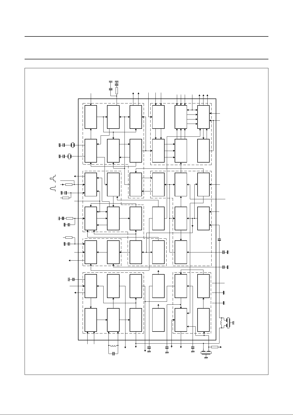
Fig.2 Block diagram for TDA8361.
Philips Semiconductors Objective specification
Integrated PAL and PAL/NTSC TV
processors
DET
R-Y output
30
DETECTOR
MANAGER
OSCILLATOR
DIVIDER
sandcastle
FBI/SCO
flyback
PH2LF
PH1LF
VRAMP
XTAL1 XTAL2
VOUT
HUE
XTALOUT
HOUT
VSTART
VFB
36 39 38 37 34 35 32 2743
41 42 40
HUE
CONTROL
XTAL
OSCILLATOR
PHASE 2
PHASE 1
OUTPUT
VERTICAL
33
PHASE
SYSTEM
TUNING
LINE
VERTICAL
to
TDA4661
B-Y output
31
DEMODULATOR
KILLERS
COLOUR
DETECTOR
COINCIDENCE
H AND V
SEPARATION
RESET
POWER
from
TDA4661
B-Y input
28
29
SET
CLAMPS
MATRIX
ACC
AMPLIFIER
NOISE
DETECTOR
TDA8362
TDA8360; TDA8361; TDA8362
BIN
R-Y input
RIN
GIN
222324
CLAMP
SWITCH
MATRIX
LUMINANCE
BANDPASS
CHROMINANCE
SWITCH
CHROMINANCE
BYPASS
TRAP AND
BOUT
GOUT
181920
STAGES
OUTPUT
PWL
Y DELAY
PEAKING
SWITCH
LUMINANCE
TUNING
ROUT
MBC214 - 1
17
16 13 15 14 2526 21
12
BRIPEAKINCVBS
CON
RGBIN
SAT
EXT
INT
CVBS
CHROMA
FT
DEC
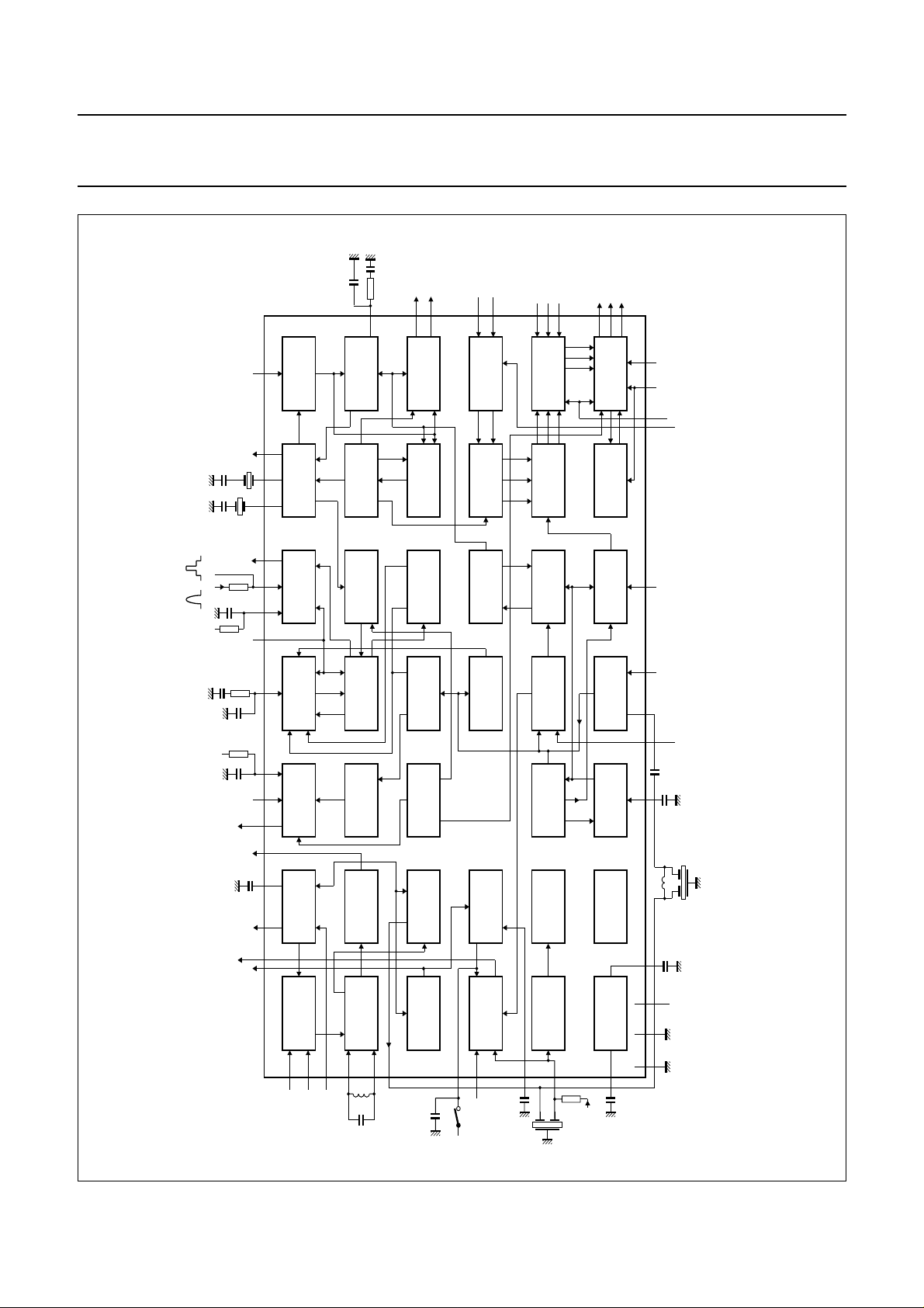
Fig.3 Block diagram for TDA8362.
AFCOUT
AGC
DEC
AGCOUT
AUOUT
IDENT
AGC
47 48 44
50
4
IF
AMPLIFIER
45
46
IFIN1
IFIN2
49
ADJ
TUNE
AFC AND
SAMPLE-
DEMODULATOR
2
IFDEM1
AND-HOLD
3
7
IFDEM2
IFOUT
VIDEO
AMPLIFIER
VIDEO
IDENTIFICATION
March 1994 6
1
MUTE
PREAMPLIFIER
SWITCH
VOLUME
6
AUDEEM
EXTAU
DEM
DEC
PLL
LIMITER
5
51
SOIF
control
volume
TEST
SUPPLY
8
DIG
DEC
910 52
11
P
V
GND2 GND1
BG
DEC
Philips Semiconductors Objective specification
Integrated PAL and PAL/NTSC TV
processors
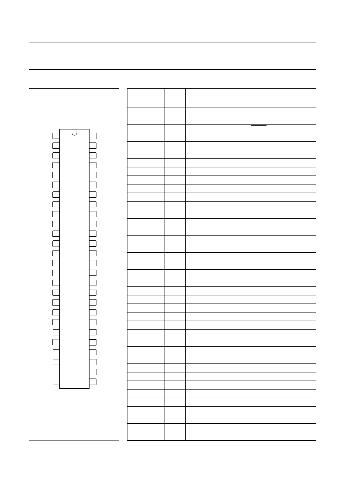
PINNING (TDA8362)
SYMBOL PIN DESCRIPTION
AUDEEM 1 audio de-emphasis and ± modulation switch
IFDEM1 2 IF demodulator tuned circuit
IFDEM2 3 IF demodulator tuned circuit
IDENT 4 video identification output/
52
51
50
49
48
47
46
45
44
43
42
41
40
39
38
37
36
35
34
33
32
31
30
29
28
27
DEC
BG
DEC
DEM
AUOUT
TUNE
ADJ
DEC
AGC
AGCOUT
IFIN2
IFIN1
AFCOUT
VOUT
VRAMP
VFB
PH1LF
PH2LF
FBI/SCO
HOUT
VSTART
XTAL2
XTAL1
DET
XTALOUT
BYO
RYO
RYI
BYI
HUE
SOIF 5 sound IF input and volume control
EXTAU 6 external audio input
IFOUT 7 IF video output
DEC
DIG
GND1 9 ground 1
V
P
GND2 11 ground 2
DEC
FT
CVBS
PEAKIN 14 peaking control input
CVBS
CHROMA 16 chrominance and A/V switch input
BRI 17 brightness control input
BOUT 18 blue output
GOUT 19 green output
ROUT 20 red output
RGBIN 21 RGB insertion and blanking input
RIN 22 red input
GIN 23 green input
BIN 24 blue input
CON 25 contrast control input
SAT 26 saturation control input
HUE 27 hue control input (or chrominance output)
BYI 28 B−Y input signal
RYI 29 R−Y input signal
RYO 30 R−Y output signal
BYO 31 B−Y output signal
XTALOUT 32 4.43 MHz output for TDA8395
DET 33 loop filter burst phase detector
XTAL1 34 3.58 MHz crystal connection
XTAL2 35 4.43 MHz crystal connection
VSTART 36 supply/start horizontal oscillator
HOUT 37 horizontal output
FBI/SCO 38 flyback input/sandcastle output
PH2LF 39 phase 2 loop filter
PH1LF 40 phase 1 loop filter
IDENT
SOIF
IFOUT
DIG
GND1
V
GND2
FT
INT
EXT
BRI
BOUT
GOUT
ROUT
RIN
GIN
BIN
CON
SAT
1
2
3
4
5
6
7
8
9
10
P
11
12
13
TDA8362
14
15
16
17
18
19
20
21
22
23
24
25
26
MBC203
AUDEEM
IFDEM1
IFDEM2
EXTAU
DEC
DEC
CVBS
PEAKIN
CVBS
CHROMA
RGBIN
Fig.4 Pin configuration for
TDA8362.
INT
EXT
TDA8360; TDA8361; TDA8362
MUTE input
8 decoupling digital supply
10 supply voltage (+8 V)
12 decoupling filter tuning
13 internal CVBS input
15 external CVBS input
March 1994 7

Philips Semiconductors Objective specification
Integrated PAL and PAL/NTSC TV
processors
SYMBOL PIN DESCRIPTION
VFB 41 vertical feedback input
VRAMP 42 vertical ramp generator
VOUT 43 vertical output
AFCOUT 44 AFC output
IFIN1 45 IF input 1
IFIN2 46 IF input 2
AGCOUT 47 tuner AGC output
DEC
AGC
TUNE
ADJ
AUOUT 50 audio output
DEC
DEM
DEC
BG
TDA8360
The TDA8360 has the following
differences to the pinning:
Pin 6: external audio input not
connected
Pin 15: external CVBS input not
connected
Pin 16: chrominance and A/V switch
input not connected
Pin 27: hue control input not
connected.
TDA8361
The TDA8361 has the following
differences to the pinning:
Pin 1: only audio de-emphasis
Pin 27: only hue control
Pin 32: 4.43 MHz output for TDA8395
is not connected.
FUNCTIONAL DESCRIPTION
Video IF amplifier
The IF amplifier contains
3 AC-coupled control stages with a
total gain control range of greater
than 60 dB. The sensitivity of the
circuit is comparable with that of
modern IF ICs.
48 AGC decoupling capacitor
49 tuner take-over adjustment
51 decoupling sound demodulator
52 decoupling bandgap supply
The reference carrier for the video
demodulator is obtained by means of
passive regeneration of the picture
carrier. The external reference tuned
circuit is the only remaining
adjustment of the IC.
In the TDA8362 the polarity of the
demodulator can be switched so that
the circuit is suitable for both positive
and negative modulated signals.
The AFC circuit is driven with the
same reference signal as the video
demodulator. To ensure that the
video content does not disturb the
AFC operation a sample-and-hold
circuit is incorporated; the capacitor
for this function is internal. The AFC
output voltage is 6 V.
The AGC detector operates on levels,
top sync for negative modulated and
top white for positive modulated
signals.The AGC detector time
constant capacitor is connected
externally. This is mainly because of
the flexibility of the application.
The time constant of the AGC system
during positive modulation
(TDA8362) is slow, this is to avoid any
visible picture variations. This,
however, causes the system to react
very slowly to sudden changes in the
input signal amplitude.
TDA8360; TDA8361; TDA8362
To overcome this problem a speed-up
circuit has been included which
detects whether the AGC detector is
activated every frame period. If,
during a 3-frame period, no action is
detected the speed of the system is
increased. When the incoming signal
has no peak white information (e.g.
test lines in the vertical retrace period)
the gain would be video signal
dependent. To avoid this effect the
circuit also contains a black level
AGC detector which is activated when
the black level of the video signal
exceeds a certain level.
The TDA8361 and TDA8362 contain
a video identification circuit which is
independent of the synchronization
circuit. Therefore search tuning is
possible when the display section of
the receiver is used as a monitor. In
the TDA8360 this circuit is only used
for stable OSD at no signal input. In
the normal television mode the
identification output is connected to
the coincidence detector, this applies
to all three devices. The identification
output voltage is LOW when no
transmitter is identified. In this
condition the sound demodulator is
switched off (mute function). When a
transmitter is identified the output
voltage is HIGH. The voltage level is
dependent on the frequency of the
incoming chrominance signal.
March 1994 8

Philips Semiconductors Objective specification
Integrated PAL and PAL/NTSC TV
processors
Sound circuit
The sound bandpass and trap filters
have to be connected externally. The
filtered intercarrier signal is fed to a
limiter circuit and is demodulated by
means of a PLL demodulator. The
PLL circuit tunes itself automatically
to the incoming signal, consequently,
no adjustment is required.
The volume is DC controlled. The
composite audio output signal has an
amplitude of 700 mV RMS at a
volume control setting of −6 dB. The
de-emphasis capacitor has to be
connected externally. The
non-controlled audio signal can be
obtained from this pin via a buffer
stage. The amplitude of this signal is
350 mV RMS.
The TDA8361 and TDA8362 external
audio input signal must have an
amplitude of 350 mV RMS. The
audio/video switch is controlled via
the chrominance input pin.
Synchronization circuit
The sync separator is preceded by a
voltage controlled amplifier which
adjusts the sync pulse amplitude to a
fixed level. The sync pulses are then
fed to the slicing stage (separator)
which operates at 50% of the
amplitude.
The separated sync pulses are fed to
the first phase detector and to the
coincidence detector. The
coincidence detector is used for
transmitter identification and to detect
whether the line oscillator is
synchronized. When the circuit is not
synchronized the voltage on the
peaking control pin (pin 14) is LOW
so that this condition can be detected
externally. The first PLL has a very
high static steepness, this ensures
that the phase of the picture is
independent of the line frequency.
The line oscillator operates at twice
the line frequency.
The oscillator network is internal.
Because of the spread of internal
components an automatic adjustment
circuit has been added to the IC.
The circuit compares the oscillator
frequency with that of the crystal
oscillator in the colour decoder. This
results in a free-running frequency
which deviates less than 2% from the
typical value.
The circuit employs a second control
loop to generate the drive pulses for
the horizontal driver stage.
X-ray protection can be realised by
switching the pin of the second
control loop to the positive supply line.
The detection circuit must be
connected externally. When the X-ray
protection is active the horizontal
output voltage is switched to a high
level. When the voltage on this pin
returns to its normal level the
horizontal output is released again.
The IC contains a start-up circuit for
the horizontal oscillator. When this
feature is required a current of 6.5 mA
has to be supplied to pin 36. For an
application without start-up both
supply pins (10 and 36) must be
connected to the 8 V supply line.
The drive signal for the vertical ramp
generator is generated by means of a
divider circuit. The RC network for the
ramp generator is external.
Integrated video filters
The circuit contains a chrominance
bandpass and trap circuit. The filters
are realised by means of gyrator
circuits and are automatically tuned
by comparing the tuning frequency
with the crystal frequency of the
decoder.
In the TDA8361 and TDA8362 the
chrominance trap is active only when
the separate chrominance input pin is
connected to ground or to the positive
supply voltage and when a colour
signal is recognized.
TDA8360; TDA8361; TDA8362
When the pin is left open-circuit the
trap is switched off so that the circuit
can also be used for S-VHS
applications.
The luminance delay line and the
delay for the peaking circuit are also
realised by means of gyrator circuits.
Colour decoder
The colour decoder in the various ICs
contains an alignment-free crystal
oscillator, a colour killer circuit and
colour difference demodulators.
The 90° phase shift for the reference
signal is achieved internally. Because
the main differences of the 3 ICs are
found in the colour decoder the
various types will be discussed.
TDA8360
This IC contains only a PAL decoder.
Depending on the frequency of the
crystals which are connected to the IC
the decoder can demodulate all PAL
standards. Because the horizontal
oscillator is calibrated by using the
crystal frequency as a reference the
4.4 MHz crystal must be connected to
pin 35 and the 3.5 MHz crystal to
pin 34. When only one crystal is
connected to the IC the other crystal
pin must be connected to the positive
supply rail via a 47 kΩ resistor. For
applications with two 3.5 MHz
crystals both must be connected to
pin 34 and the switching between the
crystals must be made externally.
Switching of the crystals is only
allowed directly after the vertical
retrace. The circuit will indicate
whether a PAL signal has been
identified by the colour decoder via
the saturation control pin.
When two crystals are connected to
the IC the output voltage of the video
identification circuit indicates the
frequency of the incoming
chrominance signal.
March 1994 9

Philips Semiconductors Objective specification
Integrated PAL and PAL/NTSC TV
processors
The conditions are:
• Signal identified at
f
= 3.6 MHz; VO = 6 V
osc
• Signal identified at
f
= 4.4 MHz (or no colour);
osc
VO = 8 V.
This information can be used to
switch the sound bandpass filter and
trap filter.
TDA8361
This IC contains an automatic
PAL/NTSC decoder. The conditions
for connecting the reference crystals
are the same as for the TDA8360.
The decoder can be forced to PAL
when the hue control pin is connected
to the positive supply voltage via a
5kΩ or 10 kΩ resistor
(approximately). The decoder cannot
be forced to the NTSC standard. It is
also possible to see if a colour signal
is recognized via the saturation pin.
TDA8362
In addition to the possibilities of the
TDA8361, the TDA8362 can
co-operate with the SECAM add-on
decoder TDA8395.
The communication between the two
ICs is achieved via pin 32. The
TDA8362 supplies the reference
signal (4.43 MHz) for the calibration
system of the TDA8395, identification
of the colour standard is via the same
connection. When a SECAM signal is
detected by the TDA8395 the IC will
draw a current of 150 µA. When
TDA8362 has not identified a colour
signal in this condition it will go into
the SECAM mode, that means it will
switch off the R−Y and B−Y outputs
and increase the voltage level on
pin 32.
This voltage will switch off the
colour-killer in the TDA8395 and
switch on the R−Y and B−Y outputs of
the TDA8395. Forcing the system to
the SECAM standard can be
achieved by loading pin 32 with a
current of 150 µA. Then the system
manager in the TDA8362 will not
search for PAL or NTSC signals.
Forcing to NTSC is not possible.
For PAL/SECAM applications the
input signal for the TDA8395 can be
obtained from pin 27 (hue control)
when this pin is connected to the
positive supply rail via the 5 kΩ or
10 kΩ resistor. An external source
selector is required by the
TDA8395/TDA8362 combination for
PAL/SECAM/NTSC applications.
RGB output circuit
The colour difference signals are
matrixed with the luminance signal to
obtain the RGB signals. Linear
amplifiers have been chosen for the
RGB inputs so that the circuit is
suitable for incoming signals from the
SCART connector. The contrast and
brightness controls operate on
internal and external signals.
The fast blanking pin has a second
detection level at 3.5 V.
When this level is exceeded the
RGB outputs are blanked so that
“On-Screen-Display” signals can be
applied to the outputs.
The output signal has an amplitude of
approximately 4 V, black-to-white,
with nominal input signals and
nominal control settings. The nominal
black level is 1.3 V.
TDA8360; TDA8361; TDA8362
March 1994 10
Philips Semiconductors Objective specification
Integrated PAL and PAL/NTSC TV
TDA8360; TDA8361; TDA8362
processors
LIMITING VALUES
In accordance with the Absolute Maximum Rating System (IEC134).
SYMBOL PARAMETER MIN. MAX. UNIT
V
P
T
stg
T
amb
T
sol
T
j
THERMAL RESISTANCE
SYMBOL PARAMETER THERMAL RESISTANCE
R
th j-a
CHARACTERISTICS
= 8 V; T
V
P
SYMBOL PARAMETER CONDITIONS MIN. TYP. MAX. UNIT
supply voltage − 9.0 V
storage temperature −25 +150 °C
operating ambient temperature −25 +70 °C
soldering temperature for 5 s − 260 °C
maximum junction temperature (operating) − 150 °C
from junction to ambient in free air 40 K/W
= 25 °C; unless otherwise specified.
amb
Supplies
V
P
I
P
I
HOSC
supply voltage (pin 10) 7.2 8.0 8.8 V
supply current (pin 10) − 80 − mA
horizontal oscillator start current
(pin 36)
P
tot
total power dissipation including start supply − 0.7 − W
IF circuit
V
ISION IF AMPLIFIER INPUTS (PINS 45 AND 46)
V
R
C
G
V
i(rms)
I
I
cr
i(rms)
input sensitivity (RMS value) note 2
Input resistance (differential) note 3 − 2 − kΩ
Input capacitance (differential) note 3 − 3 − pF
gain control range 64 −−dB
maximum input signal (RMS value) 100 −−mV
note 1 6.5 −−mA
f
= 38.90 MHz − 70 100 µV
i
= 45.75 MHz − 70 100 µV
f
i
f
= 58.75 MHz − 70 100 µV
i
March 1994 11
 Loading...