


INTEGRATED CIRCUITS
DATA SH EET
TDA8354Q
Full bridge current driven vertical
deflection output circuit in LVDMOS
Product specification
Supersedes data of 1998 Sep 03
File under Integrated Circuits, IC02
2001 Jul 11
Philips Semiconductors Product specification
Full bridge current driven vertical
TDA8354Q
deflection output circuit in LVDMOS
FEATURES
• Few external components required
• High efficiency fully DC-coupled vertical output bridge
circuit
• Vertical flyback switch with short fall and rise times
• Built-in guard circuit
• Thermal protection circuit
• Improved EMC performance due to differential inputs
• A guard signal in zoom mode.
QUICK REFERENCE DATA
SYMBOL PARAMETER CONDITIONS MIN. TYP. MAX. UNIT
DC supply
V
P
V
flb
I
q(av)
I
Vflb(av)
supply voltage 7.5 12 18 V
flyback supply voltage 2 × VP45 68 V
average quiescent supply current during scan − 10 15 mA
average flyback supply current during scan −−10 mA
Vertical circuit
I
o(p-p)
I
i(diff)(p-p)
output current (peak-to-peak value) −−3.2 A
input current (peak-to-peak value) at pin 11 or 12 − 500 600 µA
Flyback switch
I
o(Vflb)
peak output current t ≤ 1.5 ms −−±1.6 A
Thermal data (in accordance with IEC 60747-1)
T
stg
T
amb
T
vj
storage temperature −55 − +150 °C
ambient temperature −25 − +85 °C
virtual junction temperature −−150 °C
GENERAL DESCRIPTION
The TDA8354Q is a power circuit for use in 90° and 110°
colour deflection systems for 25 to 200 Hz field
frequencies, and for 4 : 3 and 16 : 9 picturetubes. The IC
contains a vertical deflection output circuit, operating as a
high efficiency class G system. The full bridge output
circuit allows DC coupling of the deflection coil in
combination with single positive supply voltages.
The IC is constructed in a Low Voltage DMOS (LVDMOS)
process that combines bipolar, CMOS and DMOS
devices. DMOS transistors are used in the output stage
because of the absence of second breakdown.
ORDERING INFORMATION
TYPE
NUMBER
NAME DESCRIPTION VERSION
PACKAGE
TDA8354Q DBS13P plastic DIL-bent-SIL power package; 13 leads (lead length 12 mm) SOT141-6
2001 Jul 11 2
Philips Semiconductors Product specification
Full bridge current driven vertical
deflection output circuit in LVDMOS
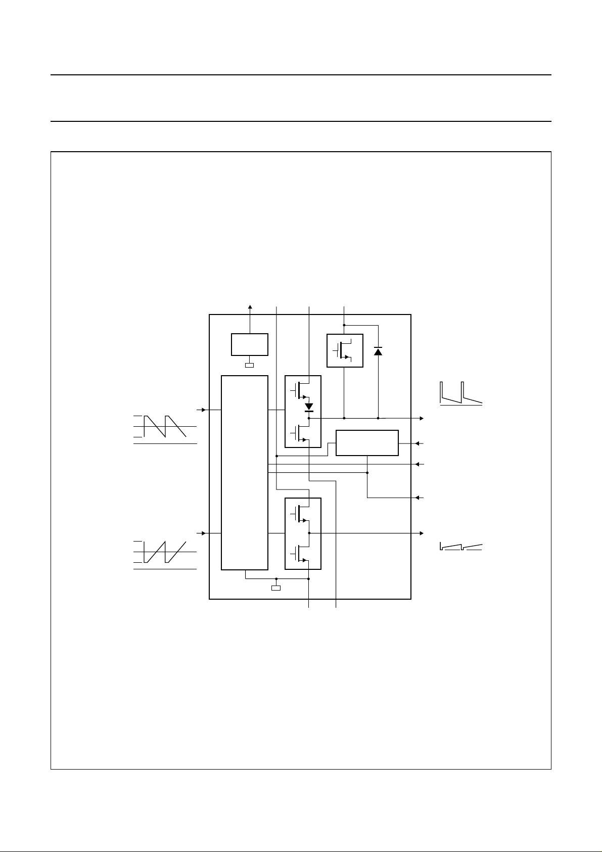
BLOCK DIAGRAM
handbook, full pagewidth
V
o(guard)
14 710
GUARD
CIRCUIT
V
P(B)VP(A)
TDA8354Q
V
flb
M1
D2
I
i(diff)
I
i(bias)
I
i(diff)
I
i(diff)
I
i(bias)
I
i(diff)
I
i(pos)
I
i(neg)
12
FEEDBACK
11
INPUT/
D3
M2
M3
M4
M5
6
GNDAGNDB
COMPENSATION
CIRCUIT
TDA8354Q
8
9
V
o(A)
13
I
i(comp)
2
V
i(M)
3
V
i(con)
5
V
o(B)
MGL461
Fig.1 Block diagram.
2001 Jul 11 3
Philips Semiconductors Product specification
Full bridge current driven vertical
deflection output circuit in LVDMOS
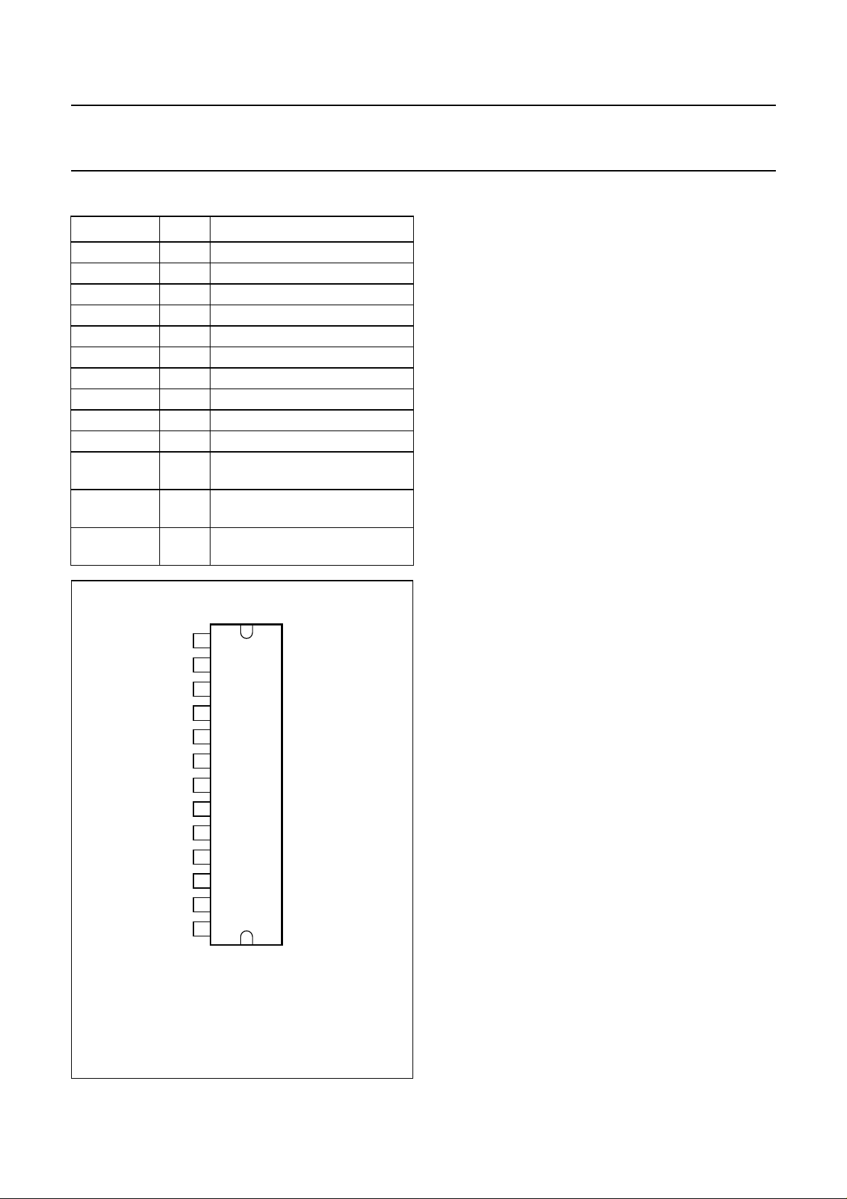
PINNING FUNCTIONAL DESCRIPTION
SYMBOL PIN DESCRIPTION
V
o(guard)
V
i(M)
V
i(con)
V
P(B)
V
o(B)
1 guard output voltage
2 input measuring resistor
3 input conversion resistor
4 supply voltage B
5 output voltage B
GNDB 6 ground B
V
flb
7 flyback supply voltage
GNDA 8 ground A
V
o(A)
V
P(A)
I
i(neg)
I
i(pos)
I
i(comp)
9 output voltage A
10 supply voltage A
11 input power stage (negative);
includes I
signal bias
i(sb)
12 input power stage (positive);
includes I
signal bias
i(sb)
13 input for damping resistor
compensation current
Vertical output stage
The vertical driver circuit has a bridge configuration, with
the deflection coil connected between the complimentary
driven output amplifiers. The differential input circuit is
current driven, and is specially designed for direct
connectiontodriver circuits delivering a differential current
signal. However, it is also suitable for single-ended input
signals.
The current to voltage conversion is done by the external
resistor (R
) connected between the output of the input
con
conversion stage and output stage B. This voltage is
compared with the output current through the deflection
coil, measured as a voltage across RM, which provides
internal feedback information. The relationship between
the differential input current and the output current is
defined by:
2 × I
i(diff)
× R
con=Icoil
× R
M
The output current is determined by the value of R
should measure 0.5 to 3.2 A (peak-to-peak value). The
allowable input current range is 50 to 800 µA for each
input.
TDA8354Q
con
and
handbook, halfpage
Thediehasbeen gluedto themetal blockof thepackage. Ifthe metal
block is not insulated from the heat sink, the heat sink may only be
connected directly to pin 6 and pin 8.
V
o(guard)
V
i(con)
V
V
GNDB
GNDA
V
V
I
i(neg)
I
i(pos)
I
i(comp)
V
P(B)
P(A)
i(M)
o(B)
V
o(A)
flb
1
2
3
4
5
6
TDA8354Q
7
8
9
10
11
12
13
MGL462
Flyback supply
The flyback voltage is determined by an additional supply
voltage V
. The principle of operating with two supply
flb
voltages(class G)makesitpossibletooptimizethesupply
voltage VP for the scan voltage and optimize the second
supply voltage V
for the flyback voltage. Using this
flb
method, very high efficiency is achieved. The supply
voltage V
is almost totally available as flyback voltage
flb
across the coil, because of the absence of a coupling
capacitor (which is not necessary as a result of the bridge
configuration). The very short rise and fall times of the
flyback switch are >400 V/µs.
Protection
The output circuit has protection circuits for:
• Too high die temperature
• Overvoltage of output stage A.
Fig.2 Pin configuration.
2001 Jul 11 4

Philips Semiconductors Product specification
Full bridge current driven vertical
deflection output circuit in LVDMOS
Guard circuit
A guard circuit with output signal V
The guard circuit generates an active HIGH level during
the flyback period. The guard circuit is also activated for
one or more of the following conditions:
• When the thermal protection is activated (Tj≈ 170 °C)
• During short circuit of the output pins (pins 5 and 9)
to VP or ground
• During open coil
• During open loop
• During short circuit of the input pins to VP or ground.
An active HIGH level of the guard signal is also generated
for the following conditions:
• No drive signal
• Short circuit of the coil.
However, for these events, the signal is generated via an
internaltimercircuit.Theguardsignalsetviathistimerhas
a delay of ≈120 ms. The delay time is given by the lowest
applicable field frequency.
o(guard)
is provided.
TDA8354Q
Damping resistor compensation
For HF loop stability, a damping resistor is connected
across the deflection coil. There is a large difference in
currentinthedampingresistor Rpduringscanandflyback.
The resistor current is summed to the current in the
deflection coil via the measuring resistor RM, which results
in a too low current in the deflection coil at the start of the
scan.
To reach a short settling time, the difference in the current
during scan and flyback in the damping resistor can be
compensated by external means. For this purpose, a
resistor (R
the output of output stage A (pin 9) and pin 13 (I
For a more accurate calculation of R
R
comp
) of about 1 MΩ can be connected between
comp
, we have:
comp
V
– VP–()R
flbVloss
=
------------------------------------------------------------------------------V
– ILRL×–()R
flbVloss
×R
×
p
con
×
M
comp
).
The guard signal can be used to blank the picture tube
screen and signal a fault condition. The guard signal can
also be used as a vertical synchronisation input pulse for
an On Screen Display (OSD) microcontroller.
2001 Jul 11 5
 Loading...