

Philips tda8350q DATASHEETS

INTEGRATED CIRCUITS
DATA SH EET
TDA8350Q
DC-coupled vertical deflection and
East-West output circuit
Product specification
Supersedes data of January 1995
File under Integrated Circuits, IC02
1999 Sep 27

Philips Semiconductors Product specification
DC-coupled vertical deflection and
TDA8350Q
East-West output circuit
FEATURES
• Few external components
• Highly efficient fully DC-coupled vertical output bridge
circuit
• Vertical flyback switch
• Guard circuit
• Protection against:
– short-circuit of the output pins
– short-circuit of the output pins to V
P
• High EMC immunity due to common mode inputs
• Temperature protection
• East-West output stage with one single conversion
resistor.
QUICK REFERENCE DATA
SYMBOL PARAMETER CONDITIONS MIN. TYP. MAX. UNIT
GENERAL DESCRIPTION
The TDA8350Q isa power circuit for use in 90° and 110°
colour deflection systems for field frequencies of 50
to 120 Hz. The circuit provides a DC driven vertical
deflection output circuit, operating as a highly efficient
class G system and an East-West driver for sinking the
diode modulator current.
DC supply
V
P
I
P
supply voltage 9 − 25 V
quiescent current − 30 − mA
Vertical circuit
I
O(p-p)
I
diff(p-p)
V
diff(p-p)
output current (peak-to-peak value) −−3A
differential input current (peak-to-peak value) − 600 −µA
differential input voltage (peak-to-peak value) − 1.5 1.8 V
Flyback switch
I
M
V
FB
peak output current −−±1.5 A
flyback supply voltage −−50 V
East-West amplifier
I
O(sink)
V
O(sink)
I
bias
output current (sink only) −−500 mA
peak output voltage I
input bias current −−1µA
Thermal data (in accordance with IEC 747-1)
T
stg
T
amb
T
vj
storage temperature −65 − 150 °C
operating ambient temperature −25 − +75 °C
virtual junction temperature −−150 °C
note 1 −−60 V
=10µA −−40 V
O(sink)
Note
1. Aflybacksupply voltage of >50 V up to 60 Visallowed in application. A 220 nF capacitor inserieswitha 22 Ω resistor
(depending on IO and the inductance of the coil) has to be connected between pin 9 and ground. The decoupling
capacitor of VFB has to be connected between pin 8 and pin 4. This supply voltage line must have a resistance of
33 Ω (see application circuit Fig.5).
1999 Sep 27 2
Philips Semiconductors Product specification
DC-coupled vertical deflection and
TDA8350Q
East-West output circuit
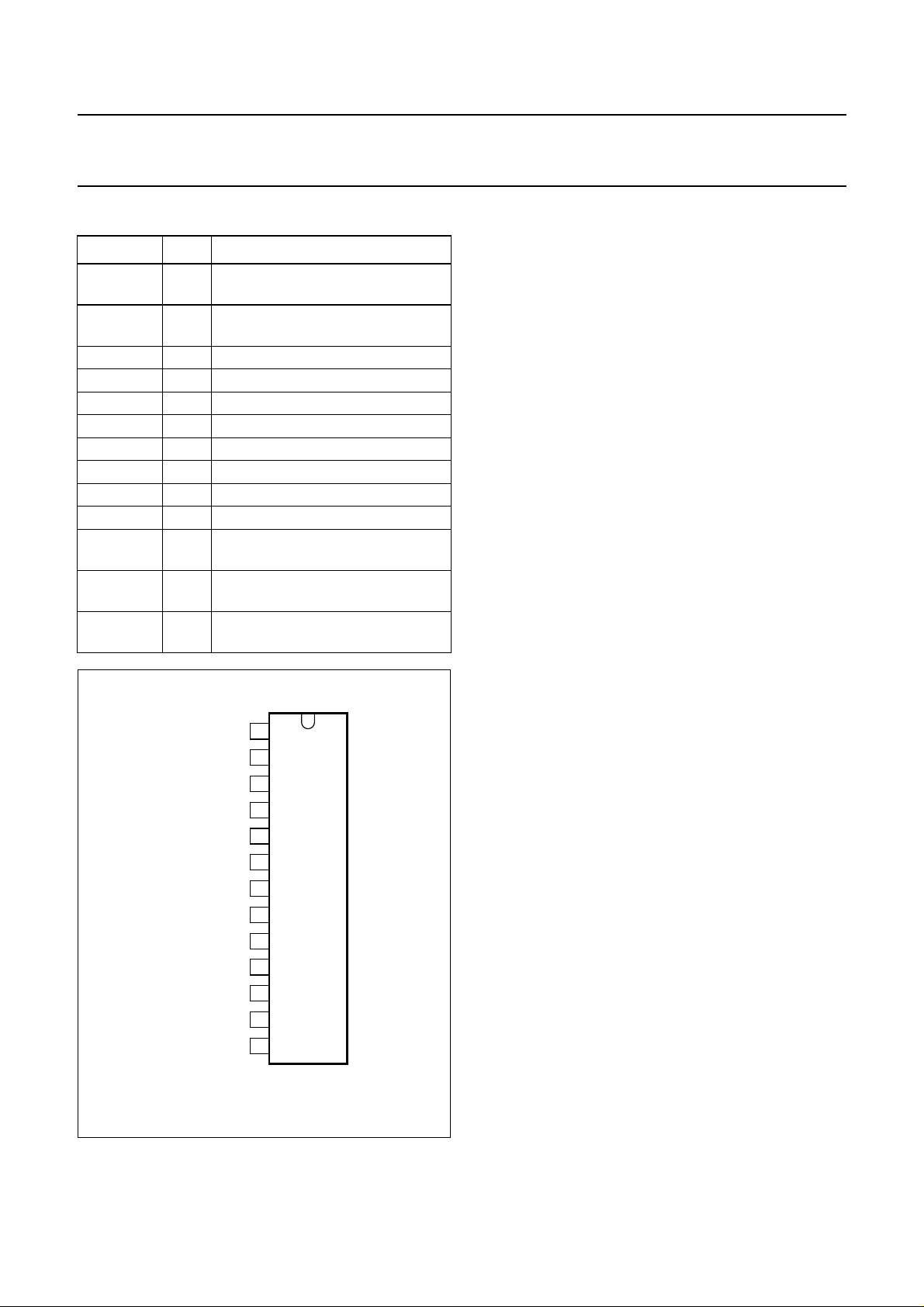
ORDERING INFORMATION
TYPE NUMBER
NAME DESCRIPTION VERSION
TDA8350Q DBS13P plastic DIL-bent-SIL power package; 13 leads (lead length 12 mm) SOT141-6
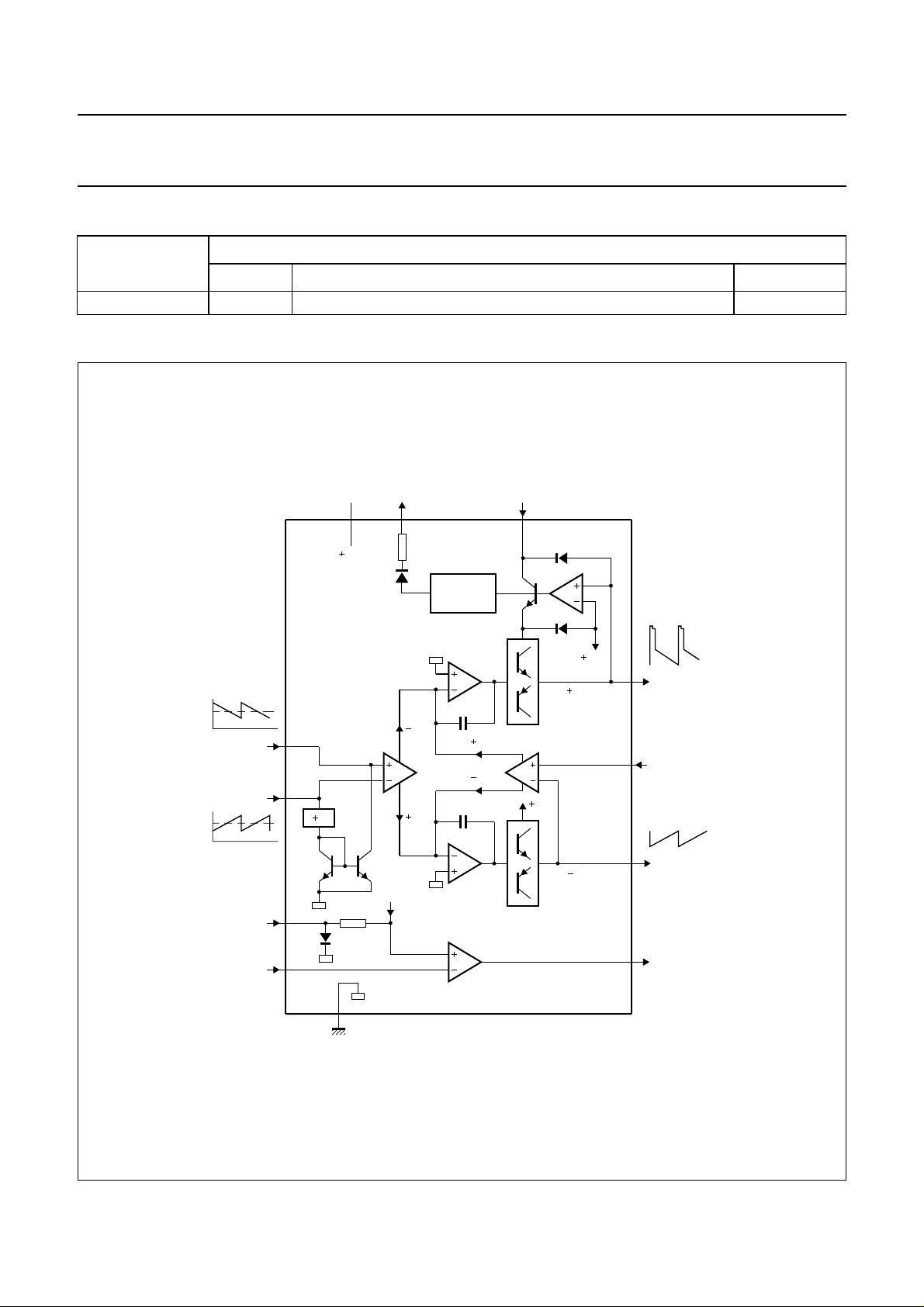
BLOCK DIAGRAM
V
handbook, full pagewidth
V
P
O(guard)
4
V
P
10
CURRENT
SOURCE
PACKAGE
V
FB
8
I
drive(pos)
I
drive(neg)
I
I(set)
I
I(corr)
1
2
13
12
TDA8350
V
7
GND
I
I(set)
V
P
9
V
V
O(A)
I
S
I
S
I
T
I
T
V
P
V
O(B)
11
MBC229-1
O(A)
3
V
I(fb)
5
V
O(B)
V
O(sink)
Fig.1 Block diagram.
1999 Sep 27 3
Philips Semiconductors Product specification
DC-coupled vertical deflection and
East-West output circuit
PINNING FUNCTIONAL DESCRIPTION
SYMBOL PIN DESCRIPTION
I
drive(pos)
I
drive(neg)
V
I(fb)
V
P
V
O(B)
1 input power-stage (positive);
includes I
signal bias
I(sb)
2 input power-stage (negative);
includes I
signal bias
I(sb)
3 feedback voltage input
4 supply voltage
5 output voltage B
n.c. 6 not connected
GND 7 ground
V
FB
V
O(A)
V
O(guard)
V
O(sink)
8 flyback supply voltage
9 output voltage A
10 guard output voltage
11 East-West amplifier driver (sink)
output voltage
I
I(corr)
12 East-West amplifier input
correction current (negative)
I
I(set)
13 East-West amplifier set input
current (positive)
handbook, halfpage
I
drive(pos)
I
drive(neg)
V
V
O(B)
GND
V
V
O(A)
V
O(guard)
V
O(sink)
I
I(corr)
I
I(set)
I(fb)
V
n.c.
FB
1
2
3
4
P
5
6
7
TDA8350
8
9
10
11
12
13
MBC226-1
Fig.2 Pin configuration.
The vertical driver circuit is a bridge configuration. The
deflectioncoilisconnectedbetweentheoutputamplifiers,
which are driven in opposite phase. An external resistor
(RM) connected in series with the deflection coil provides
internal feed back information. The differential input
circuit is voltage driven. The input circuit has been
adapted to enable it to be used with the TDA9150,
TDA9151B, TDA9160A, TDA9162, TDA8366 and
TDA8367 which deliver symmetrical current signals. An
external resistor (R
) connected between the
CON
differential input determines the output current through
the deflection coil. The relationship between the
differential input current and the output current is defined
by: I
diff
× R
CON=I(coil)
× RM. The output current is
adjustable from 0.5 A (p-p) to 3 A (p-p) by varying RM.
The maximum input differential voltage is 1.8 V. In the
applicationit is recommended thatV
is recommended because of the spread of input current
and the spread in the value of R
The flyback voltage is determined byan additional supply
voltage VFB. The principle of operating with two supply
voltages (class G) makes it possible to fix the supply
voltage VPoptimum for the scan voltage and the second
supplyvoltage VFBoptimumfor the flyback voltage. Using
this method, very high efficiency is achieved.
The supply voltage VFB is almost totally available as
flyback voltage across the coil, this being possible due to
the absence of a decoupling capacitor (not necessary,
due to the bridge configuration). Built-in protections are:
• thermal protection
• short-circuit protection of the output pins (pins 5 and 9)
• short-circuit protection of the output pins to V
A guard circuit V
is provided. The guard circuit is
O(guard)
activated at the following conditions:
• during flyback
• during various short-circuit possibilities at the output
pins
• during open loop
• when the thermal protection is activated.
This signal can be used for blanking the picture tube
screen.
An East-West amplifier is also provided. This amplifier is
an inverting amplifier which is current driven. The output
is a current sink.
TDA8350Q
= 1.5 V (typ). This
diff
.
CON
P.
1999 Sep 27 4

Philips Semiconductors Product specification
DC-coupled vertical deflection and
TDA8350Q
East-West output circuit
LIMITING VALUES
In accordance with the Absolute Maximum Rating System (IEC 134).
SYMBOL PARAMETER CONDITIONS MIN. MAX. UNIT
DC supply
V
P
V
FB
Vertical circuit
I
O
V
O(A)
Flyback switch
I
M
East-West amplifier
V
O(sink)
I
O(sink)
Thermal data (in accordance with IEC 747-1)
T
stg
T
amb
T
vj
R
th vj-c
R
th vj-a
t
sc
supply voltage non-operating − 40 V
− 25 V
flyback supply voltage − 50 V
note 1 60 V
output current (peak-to-peak value) note 2 − 3A
output voltage (pin 9) − 52 V
note 1 62 V
peak output current −±1.5 A
output voltage I
output current V
=10µA; note 3 − 40 V
O(sink)
= 2 V; note 3 − 500 mA
O(sink)
storage temperature −65 150 °C
operating ambient temperature −25 +75 °C
virtual junction temperature − 150 °C
resistance vj-case − 4 K/W
resistance vj-ambient in free air − 40 K/W
short-circuiting time note 4 − 1hr
Notes
1. Aflybacksupply voltage of >50 V up to 60 Visallowed in application. A 220 nF capacitor inserieswitha 22 Ω resistor
(depending on I
and the inductance of the coil) has to be connected between pin 9 and ground. The decoupling
O
capacitor of VFB has to be connected between pin 8 and pin 4. This supply voltage line must have a resistance of
33 Ω (see application circuit Fig.5).
2. IO maximum determined by current protection.
3. The operating area is limited by a straight line between the points V
I
= 500 mA.
O(sink)
O(sink)
=40V;I
=10µA and V
O(sink)
O(sink)
=2V;
4. Up to Vp=18V.
1999 Sep 27 5
 Loading...