

Philips TDA8340 Service Manual

INTEGRATED CIRCUITS
DATA SH EET
TDA8340
TDA8341
Television IF amplifier and
demodulator
Product specification
File under Integrated Circuits, IC02
November 1987

Philips Semiconductors Product specification
Television IF amplifier and demodulator
DESCRIPTION
The TDA8340;Q and TDA8341;Q are integrated IF
amplifier and demodulator circuits for colour or black/white
television receivers, the TDA8340;Q is for application with
n-p-n tuners and the TDA8341;Q for p-n-p tuners.
The TDA8340;Q and TDA8341;Q are pin-compatible
successors with improved performance to types
TDA2540/2541;Q and TDA3540/3541;Q.
TDA8340
TDA8341
Features
• Full range gain-controlled wide-band IF amplifier
• Linear synchronous demodulator with excellent
intermodulation performance
• White spot inverter
• Wide-band video amplifier with noise protection
• AFC circuit with AFC on/off switching and
sample-and-hold function
• Low impedance AFC output
• AGC circuit with noise gating
• Tuner AGC output for n-p-n tuners (TDA8340) or p-n-p
tuners (TDA8341)
• External video switch for switching-off the video output
• Reduced sensitivity for high sound carriers
• Integrated filter to limit second harmonic IF signals
• Wide supply voltage range
• Requires few external components
QUICK REFERENCE DATA
PARAMETER CONDITIONS SYMBOL MIN. TYP. MAX. UNIT
Supply voltage (pin 11) V
Supply current (pin 11) I
CC=V11-13
11
9,4 12 13,2 V
30 42 55 mA
IF input sensitivity
(r.m.s. value) V
IF gain control range G
1-16(rms)
v
20 40 80 µV
− 67 − dB
Video output voltage white signal;
(peak-to-peak value) 10% top sync V
Signal-to-noise ratio V
= 10 mV S/(S+N) 50 58 − dB
i
12−13(p−p)
2,4 2,7 3,0 V
AFC output voltage swing
(peak-to-peak value) V
5-13(p-p)
− 10 − V
PACKAGE OUTLINES
TDA8340; TDA8341: 16-lead DIL; plastic (SOT38); SOT38-1; 1996 november 29.
November 1987 2
Philips Semiconductors Product specification
Television IF amplifier and demodulator
TDA8340
TDA8341
November 1987 3
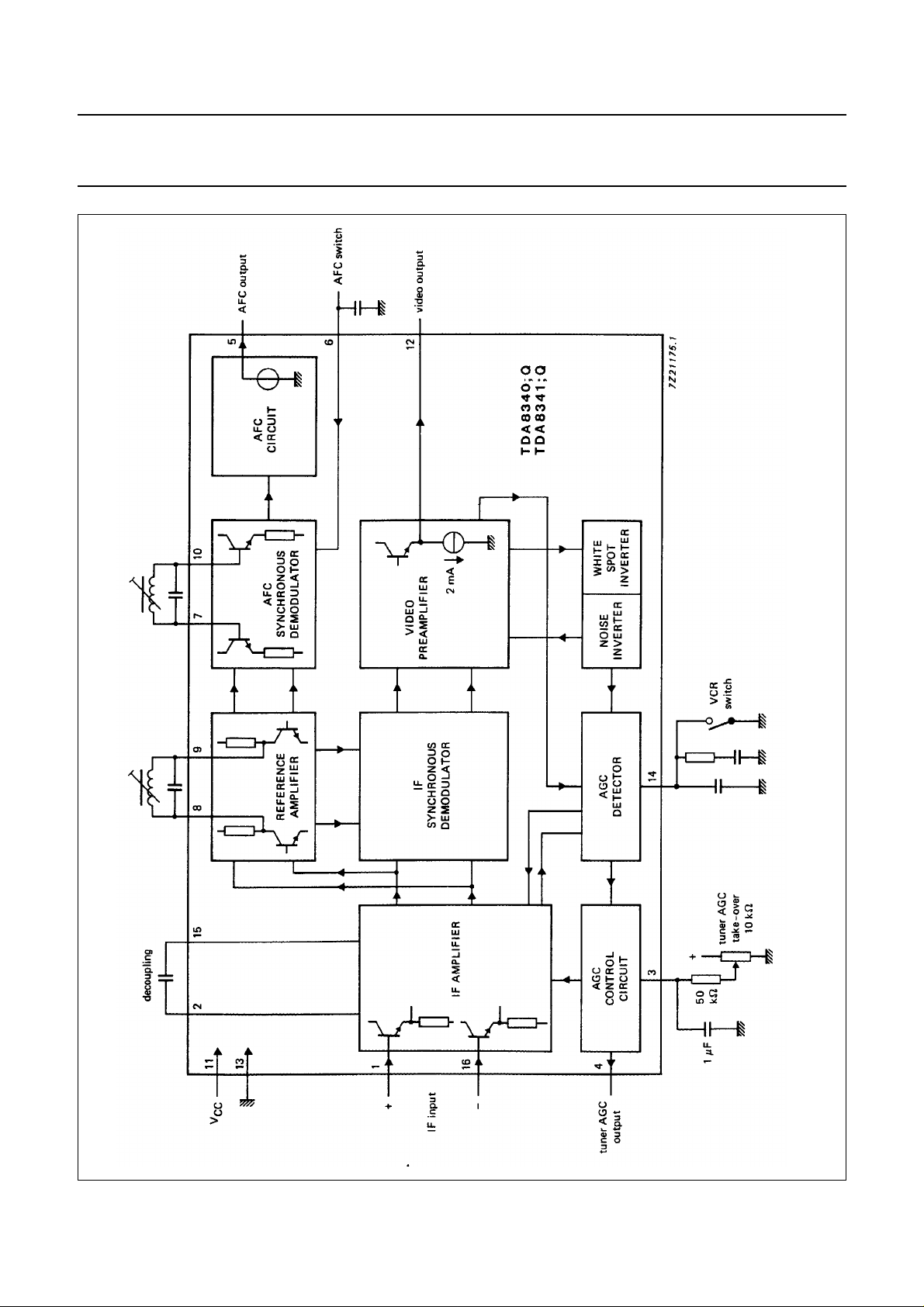
Fig.1 Block diagram.

Philips Semiconductors Product specification
Television IF amplifier and demodulator
PINNING
1 and 16 Balanced IF inputs
2 and 15 IF amplifier decoupling
3 Tuner AGC starting point adjustment
4 Tuner AGC output
5 AFC output
6 AFC on/off switch and sample-and-hold capacitor
7 and 10 Reference carrier π/2 rad. phase shift
8 and 9 IF picture carrier passive regeneration
11 Positive supply voltage (V
12 Video output
13 Ground (V
14 IF AGC capacitor and VCR switch
FUNCTIONAL DESCRIPTION
IF amplifier
EE
)
CC
)
TDA8340
TDA8341
This is a 3-stage, gain-controlled IF amplifier with a wide dynamic range. On-chip capacitors in the d.c. feedback loop of
the amplifier maintain stability at maximum gain. Internal stabilization of the supply voltage ensures the desired sensitivity
and gain control range over the whole supply voltage range and also gives very good power supply ripple rejection in this
part of the circuit.
Demodulator
The redesigned IF demodulator is a quasi-synchronous circuit that employs passive carrier regeneration and logarithmic
clamping to give improved signal handling. The demodulator input is a.c. coupled to the IF amplifier to reduce d.c. offsets
and thus minimize residual IF carrier in the output signal.
Video amplifier
The linearity and bandwidth of the video amplifier are sufficient to meet all wide band requirements, e.g. for teletext
transmissions. Second harmonics of the IF carrier are effectively reduced by a Sallen-Key low pass interstage filter
between the demodulator output and the video amplifier input. An integrated filter in the noise inverter reduces the
sensitivity of the video amplifier for high sound carriers.
White spot protection comprises a white spot clamp system combined with a delayed-action inverter which is also highly
resistant to high sound carriers.
Note. To prevent radiated video output at the input pins, connect a 6,8 µH inductor in series with pin 12 and fit as close
as possible to the IC body. Use short leads.
AGC detector
A Bessel low-pass filter between the video output and the AGC detector improves the detector function in the presence
of high sound carriers. No ‘hang-up’ occurs in the detector after pin 14 has been short-circuited to ground (VCR switch
operated). The detector also generates the sample-and-hold pulse for the AFC system.
November 1987 4

Philips Semiconductors Product specification
Television IF amplifier and demodulator
TDA8340
TDA8341
AGC control circuit
This converts the AGC detector voltage (pin 14) into a current signal which controls the gain of the IF amplifier. It also
provides a tuner AGC control output from pin 4, current limiting is incorporated to prevent internal damage. The AGC
starting point is adjusted via pin 3.
AFC circuit
The AFC circuit provides a voltage output which controls the IF frequency of the tuner. Video information on the AFC
output (pin 5) is eliminated by a sample-and-hold circuit (external capacitor at pin 6). Coupling between the AFC and
reference tuned circuits is via two small capacitors (or parasitic capacitance) between the respective tracks of the printed
circuit board. If the capacitance is less than 1 pF, the steepness of the AFC characteristic is reduced.
RATINGS
Limiting values in accordance with the Absolute Maximum System (IEC 134)
PARAMETER SYMBOL MIN. MAX. UNIT
Supply voltage (pin 11) V
IF AGC voltage/VCR switch V
Tuner AGC voltage V
AFC switch voltage V
Maximum voltage level with
VCR switch active V
DC current at video output I
DC current at AFC output I
Total power dissipation P
Storage temperature range T
Operating ambient temperature T
CC=V11−13
14-13
4-13
6-13
12-13
12
5
tot
stg
amb
9,4 13,2 V
− 13,2 V
− 12 V
− 13,2 V
− 5,0 V
− 10 mA
− 10 mA
− 1,2 W
−55 +150 °C
−25 +70 °C
November 1987 5
 Loading...