Philips tda8315t DATASHEETS

INTEGRATED CIRCUITS
DATA SH EET
TDA8315T
Integrated NTSC decoder
and sync processor
Preliminary specification
File under Integrated Circuits, IC02
Philips Semiconductors
September 1994

Philips Semiconductors Preliminary specification
Integrated NTSC decoder
TDA8315T
and sync processor
FEATURES
• CVBS or Y/C input
• Integrated chrominance trap and bandpass filters
(automatically calibrated)
• Integrated luminance delay line
• Alignment-free NTSC colour decoder
• Horizontal PLL with an alignment-free horizontal
oscillator
• Vertical count-down circuit
• Low dissipation (320 mW)
• Small amount of peripheral components compared with
competition ICs.
QUICK REFERENCE DATA
SYMBOL PARAMETER MIN. TYP. MAX. UNIT
V
P
I
P
supply voltage (pins 11 and 12) 7.2 8.0 8.8 V
supply current − 40 − mA
Input voltages
V
13(p-p)
V
15(p-p)
CVBS/Y input voltage (peak-to-peak value) − 1 − V
chrominance input voltage (peak-to-peak value) − 0.3 − V
Output signals
V
O(b-w)
V
21(p-p)
V
20(p-p)
V
2
V
7
V
10
luminance output voltage (blank-to-white value) − 1.65 − V
−U output voltage (peak-to-peak value) − 1.5 − V
−V output voltage (peak-to-peak value) − 1.5 − V
horizontal sync pulse − 4 − V
vertical sync pulse − 4 − V
back porch clamping pulse − 4 − V
Control voltages
V
control
control voltages for Saturation and Hue 0 − 5V
GENERAL DESCRIPTION
The TDA8315T is an alignment-free NTSC decoder/sync
processor. The device can be used for normal television
applications and for Picture-in-Picture (PIP) applications.
The input signal can be either CVBS or Y/C and at the
outputs the following signals are available:
Luminance signal
Colour difference signals (U and V)
Horizontal and vertical synchronization pulses
Back porch clamping pulse (burst-key pulse).
The supply voltage for the IC is 8 V. It is available in a
24-pin SO package.
ORDERING INFORMATION
TYPE NUMBER
TDA8315T SO24 plastic small outline package; 24 leads; body width 7.5 mm SOT137-1
September 1994 2
PACKAGE
NAME DESCRIPTION VERSION

Philips Semiconductors Preliminary specification
Integrated NTSC decoder
and sync processor
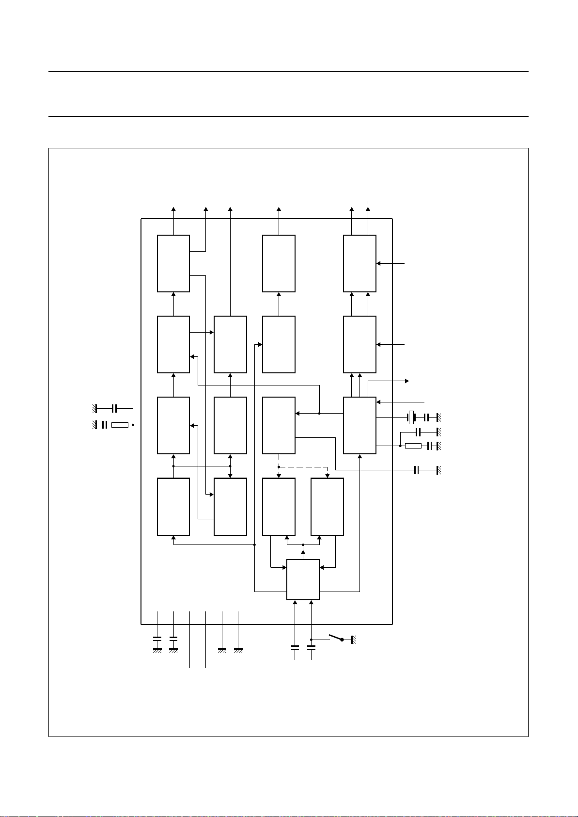
BLOCK DIAGRAM
HOUT
2
PULSE
SHAPER
PLUS
CONTROL
OSCILLATOR
CLAMP
10
VOUT
7
H/V DIVIDER
Y
19
AMPLIFIER
DELAY LINE
LUMINANCE
V
U
20
21
CONTROL
SATURATION
MATRIX
U/V-SIGNALS
TDA8315T
MBE015
SAT
816
SW
PH1LF
SSC DEM
reference
4
PHASE
DETECTOR
SYNC
SEPARATOR
SYNC
VERTICAL
SEPARATOR
DETECTOR
COINCIDENCE
FILTER
TUNING
TRAP
CHROMINANCE
CHROMINANCE
NTSC
DECODER
14 22 24 18 17
BANDPASS
HUE
PLL XTAL
FT
DEC
handbook, full pagewidth
Fig.1 Block diagram.
TDA8315T
CVBS/Y
SWITCH
9
DIG
DEC
5
BG
DEC
11
12
3
23
P1
P2
V
GND1
V
GND2
13
CVBS
15
CHROMA
CVBS/Y
switch
September 1994 3

Philips Semiconductors Preliminary specification
Integrated NTSC decoder
and sync processor
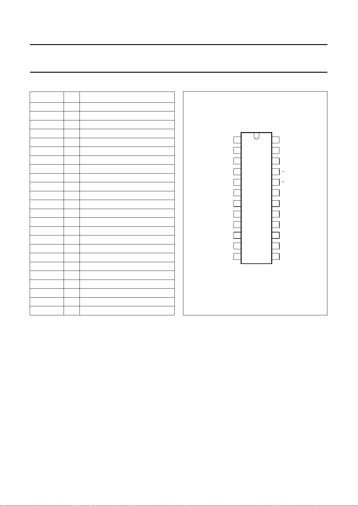
PINNING
SYMBOL PIN DESCRIPTION
(1)
TEST1
HOUT 2 horizontal output pulse
GND1 3 ground 1 (0 V)
PH1LF 4 phase 1 loop filter
DEC
BG
(1)
TEST2
VOUT 7 vertical output pulse
DEM
SW
DEC
DIG
CLAMP 10 back porch clamping pulse
V
P1
V
P2
CVBS/Y 13 CVBS/Y input
DEC
FT
CHROMA 15 chrominance and switch input
SAT 16 saturation control input
SCS 17 sub-carrier signal output
HUE 18 hue control input
Y 19 Y output
−V20−V output
−U21−U output
PLL 22 PLL colour filter
GND2 23 ground 2 (0 V)
XTAL 24 3.58 MHz crystal connection
1 test pin 1
5 bandgap decoupling
6 test pin 2
8 demodulation angle switch
9 decoupling digital supply
11 supply voltage 1 (+8 V)
12 supply voltage 2 (+8 V)
14 decoupling filter tuning
handbook, halfpage
HOUT
GND1
DEC
VOUT
SW
DIG
V
P1
V
P2
1
2
3
4
5
6
TDA8315T
7
8
9
10
11
12
TEST1
PH1LF
BG
TEST2
DEM
DEC
CLAMP
Fig.2 Pin configuration.
MBE016
TDA8315T
XTAL
24
GND2
23
PLL
22
21
U
V
20
19
Y
18
HUE
SCS
17
SAT
16
CHROMA
15
DEC
14
13
FT
CVBS/Y
Note
1. In the application the test pins must be connected to
ground.
September 1994 4

Philips Semiconductors Preliminary specification
Integrated NTSC decoder
and sync processor
FUNCTIONAL DESCRIPTION
CVBS or Y/C input
The TDA8315T has a video input which can be switched
to CVBS (with internal chrominance bandpass and trap
filters) and to Y/C (without chrominance bandpass and
trap filters). The switching between CVBS and Y/C is
achieved by the DC level of the CHROMA input (pin 15).
Integrated video filters
The circuit contains a chrominance bandpass and trap
circuit. The filters are realised by gyrator circuits that are
automatically tuned by comparing the tuning frequency
with the crystal frequency of the decoder. The
chrominance trap can be switched off by the DC level of
the CHROMA input.
The luminance delay line is also realised by gyrator
circuits.
Colour decoder
The colour decoder contains an alignment-free crystal
oscillator, a colour killer circuit and colour difference
demodulators. The gain of the two colour difference signal
demodulators is identical and the phase angle of the
reference carrier signals is 90°. This phase shift is
achieved internally. It is possible to switch the demodulator
angle to 110° by an internal matrix circuit. The switching is
obtained externally via pin 8.
TDA8315T
Synchronization circuit
The sync separator is preceded by a voltage controlled
amplifier which adjusts the sync pulse amplitude to a fixed
level. The sync pulses are then fed to the slicing stage
(separator) which operates at 50% of the amplitude.
The separated sync pulses are fed to the first phase
detector and to the coincidence detector. The coincidence
detector is used to detect whether the line oscillator is
synchronized. The PLL has a very high static steepness,
this ensures that the phase of the picture is independent of
the line frequency. The line oscillator operates at twice the
line frequency.
The oscillator network is internal. Because of the spread of
internal components an automatic adjustment circuit has
been added to the IC.
The circuit compares the oscillator frequency with that of
the crystal oscillator in the colour decoder. This results in
a free-running frequency which deviates less than 2% from
the typical value.
The horizontal output pulse is derived from the horizontal
oscillator via a pulse shaper. The pulse width of the output
pulse is 5.4 µs, the front edge of this pulse coincides with
the front edge of the sync pulse at the input.
The vertical output pulse is generated by a count-down
circuit. The pulse width is approximately 380 µs. Both the
horizontal and vertical pulses will always be available at
the outputs even when no input signal is available.
September 1994 5
 Loading...