

Philips tda8007b DATASHEETS

INTEGRATED CIRCUITS
DATA SH EET
TDA8007B
Double multiprotocol IC card
interface
Product specification
Supersedes data of 2000 Aug 29
File under Integrated Circuits, IC02
2000 Nov 09

Philips Semiconductors Product specification
Double multiprotocol IC card interface TDA8007B
FEATURES
• Control and communication through an 8-bit parallel
interface, compatible with multiplexed or
non-multiplexed memory access
• Specific ISO UART with parallel access on I/O for
automatic convention processing, variable baud rate
through frequency or division ratio programming, error
management at character level for T = 0, extra guard
time register
• 1 to 8 characters FIFO in reception mode
• Parity error counter in reception mode
• Dual VCC generation (5 V ±5%, 65 mA (max.) or 3 V
±8%, 50 mA (max.) with controlled rise and fall times)
• Dual cards clock generation (up to 10 MHz), with two
times synchronous frequency doubling
• Cards clock STOP HIGH, clock STOP LOW or
1.25 MHz (from internal oscillator) for cards
Power-down mode
• Automaticactivationanddeactivationsequencethrough
an independent sequencer
• Supports the asynchronousprotocols T = 0 and T = 1 in
accordance with ISO 7816 and EMV
• Versatile 24-bit time-out counter for Answer To Reset
(ATR) and waiting times processing
• 22 ElementaryTime Unit (ETU)counter for Block Guard
Time (BGT)
• Supports synchronous cards
• Current limitations in the event of short-circuit
• Special circuitry for killing spikes during power-on/-off
• Supply supervisor for power-on/-off reset
• Step-up converter (supply voltage from 2.7 to 6 V),
doubler, tripler or follower according to VCC and V
• Additional I/O pin allowing use of the ISO UART for
another analog interface (pin I/OAUX)
• Additional interrupt pin allowing detection of level
toggling on an external signal (pin INTAUX)
DD
• Fast and efficient swapping between the 3 cards due to
separate buffering of parameters for each card
• Chip select input allowing use of several devices in
parallel and memory space paging
• Enhanced ESD protections on card side [6 kV (min.)]
• Software library for easy integration within the
application
• Power-down mode for reducing current consumption
when no activity.
APPLICATIONS
• Multiple smart card readers for multiprotocol
applications (EMV banking, digital pay TV, access
control, etc.).
GENERAL DESCRIPTION
The TDA8007B is a low cost card interface for dual smart
card readers. Controlled through a parallel bus, it takes
care of all ISO 7816, EMV and GSM11-11 requirements.
It may be interfaced to the P0/P2 ports of a 80C51 family
microcontroller, and be addressed as a memory through
MOVX instructions. It may also be addressed on a
non-multiplexed 8-bit data bus, by means of address
registers AD0, AD1, AD2 and AD3. The integrated ISO
UART and the time-out counters allow easy use even at
high baud rates with no real time constraints. Due to its
chip select and external I/O and INT features, it greatly
simplifies the realization of any number of cards readers.
It gives the cards and the reader a very high level of
security, due to its special hardware against ESD,
short-circuiting, power failure, etc. Its integrated step-up
converterallowsoperation within a supply voltagerangeof
2.7 to 6 V.
A software library has been developed, taking care of all
actions required for T = 0, T = 1 and synchronous
protocols (see application reports).
ORDERING INFORMATION
TYPE
NUMBER
TDA8007BHL LQFP48 plastic low profile quad flat package; 48 leads; body 7 × 7 × 1.4 mm SOT313-2
2000 Nov 09 2
NAME DESCRIPTION VERSION
PACKAGE

Philips Semiconductors Product specification
Double multiprotocol IC card interface TDA8007B
QUICK REFERENCE DATA
SYMBOL PARAMETER CONDITIONS MIN. TYP. MAX. UNIT
V
DD
I
DD(pd)
I
DD(sm)
I
DD(om)
V
CC
I
CC
I
CC1+ICC2
SR slew rate on V
t
deact
t
act
f
xtal
f
op
T
amb
supply voltage 2.7 − 6V
supply current in power-down
mode
VDD= 3.3 V; cards inactive; XTAL
oscillator stopped
= 3.3 V; cards active at
V
DD
−−350 µA
−−3mA
VCC= 5 V; CLK stopped; XTAL
oscillator stopped
supply current in sleep mode cards powered at 5 V but clock
−−5.5 mA
stopped
supply current in operating mode VDD= 3.3 V; f
V
CC1=VCC2
I
CC1+ICC2
= 20 MHz;
XTAL
=5V;
=80mA
−−315 mA
output card supply voltage including static loads (5 V card) 4.75 5.0 5.25 V
with 40 nC dynamic loads on
4.6 − 5.4 V
200 nF capacitor (5 V card)
including static loads (3 V card) 2.78 − 3.22 V
with 24 nC dynamic loads on
2.75 − 3.25 V
200 nF capacitor (3 V card)
output card supply current operating; 5 V card −−65 mA
operating; 3 V card −−50 mA
overload detection − 100 − mA
sum of both cards currents −−80 mA
(rise and fall) C
CC
= 300 nF 0.05 0.16 0.22 V/µs
L(max)
deactivation cycle duration −−150 µs
activation cycle duration −−225 µs
crystal frequency 4 − 27 MHz
operating frequency external frequency applied to pin
0 − 25 MHz
XTAL1
ambient temperature −25 − +85 °C
2000 Nov 09 3

Philips Semiconductors Product specification
Double multiprotocol IC card interface TDA8007B
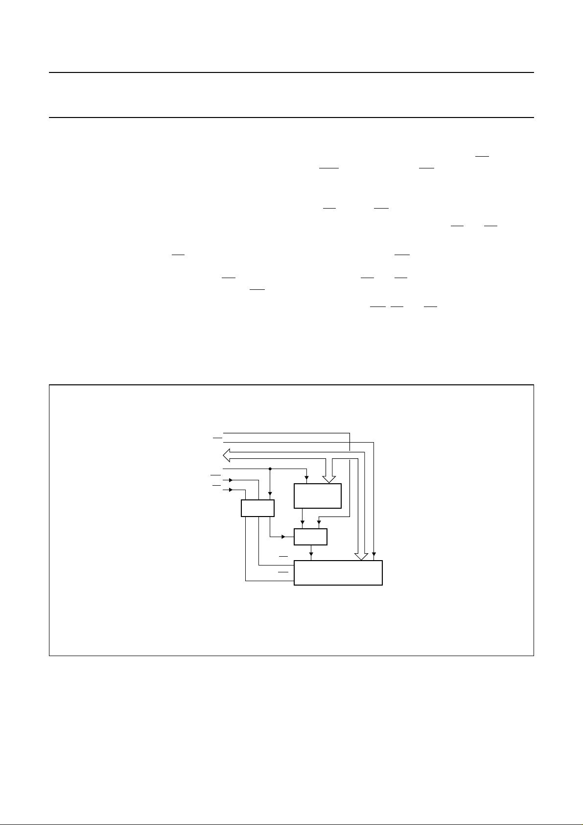
BLOCK DIAGRAM
handbook, full pagewidth
RSTOUT
DELAY
22 nF
INT
ALE
AD0
AD1
AD2
AD3
RD
WR
D0
D1
D2
D3
D4
D5
D6
D7
CS
I/OAUX
INTAUX
V
DD
100 nF
1
48
40
39
45
44
43
42
36
37
28
29
30
31
32
33
34
35
38
2
41
SUPPLY
AND
SUPERVISOR
ISO7816
UART
TIME-OUT
COUNTER
INTERFACE CONTROL
CLOCK
CIRCUIT
GND
V
DDA
220 nF
SAP SAM
STEP-UP
CONVERTER
ANALOG
DRIVERS
SEQUENCERS
AND
220 nF
SBP SBM
AGND
2524222621231927
20
6
4
8
10
9
3
5
7
14
12
16
18
17
11
13
15
V
UP
220 nF
C41
C81
CLK1
RST1
V
CC1
I/O1
PRES1
GNDC1
C42
C82
CLK2
RST2
V
CC2
I/O2
PRES2
GNDC2
TDA8007B
XTAL1 XTAL2
Fig.1 Block diagram.
2000 Nov 09 4
INT OSC
XTAL OSC
47 46
FCE534
Philips Semiconductors Product specification
Double multiprotocol IC card interface TDA8007B
PINNING
SYMBOL PIN DESCRIPTION
RSTOUT 1 open-drain output for resetting external chips
I/OAUX 2 input or output for an I/O line issued of an auxiliary smart card interface
I/O1 3 data line to/from card 1 (ISO C7 contact)
C81 4 auxiliary I/O for ISOC8 contact (synchronous cards for instance) for card 1
PRES1 5 card 1 presence contact input (active HIGH or LOW by mask option)
C41 6 auxiliary I/O for ISOC4 contact (synchronous cards for instance) for card 1
GNDC1 7 ground for card 1
CLK1 8 clock output to card 1 (ISO C3 contact)
V
CC1
RST1 10 card 1 reset output (ISO C2 contact)
I/O2 11 data line to/from card 2 (ISO C7 contact)
C82 12 auxiliary I/O for ISO C8 contact (synchronous cards for instance) for card 2
PRES2 13 card 2 presence contact input (active HIGH or LOW by mask option)
C42 14 auxiliary I/O for ISO C4 contact (synchronous cards for instance) for card 2
GNDC2 15 ground for card 2
CLK2 16 clock output to card 2 (ISO C3 contact)
V
CC2
RST2 18 card 2 reset output (ISO C2 contact)
GND 19 ground connection
V
UP
SAP 21 contact 1 for the step-up converter (connect a low ESR 220 nF capacitor between pins SAP
SBP 22 contact 3 for the step-up converter (connect a low ESR 220 nF capacitor between pins SBP
V
DDA
SBM 24 contact 4 for the step-up converter (connect a low ESR 220 nF capacitor between pins SBP
AGND 25 ground connection for the step-up converter
SAM 26 contact 2 for the step-up converter (connect a low ESR 220 nF capacitor between pins SAP
V
DD
D0 28 data 0 or add 0
D1 29 data 1 or add 1
D2 30 data 2 or add 2
D3 31 data 3 or add 3
D4 32 data 4 or add 4
D5 33 data 5 or add 5
D6 34 data 6 or add 6
D7 35 data 7 or add 7
RD 36 read selection signal (read or write in non-multiplexed configuration)
9 card 1 supply output voltage (ISO C1 contact)
17 card 2 supply output voltage (ISO C1 contact)
20 output of the step-up converter
and SAM)
and SBM)
23 positive analog supply voltage for the step-up converter
and SBM)
and SAM)
27 positive supply voltage
2000 Nov 09 5

Philips Semiconductors Product specification
Double multiprotocol IC card interface TDA8007B
SYMBOL PIN DESCRIPTION
WR 37 write selection signal (enable in case of non-multiplexed configuration)
CS 38 chip select input (active HIGH or LOW)
ALE 39 address latch enable in case of multiplexed configuration (connect toV
configuration)
INT 40 interrupt output (active LOW)
INTAUX 41 auxiliary interrupt input
AD3 42 register selection address 3
AD2 43 register selection address 2
AD1 44 register selection address 1
AD0 45 register selection address 0
XTAL2 46 connection pin for an external crystal
XTAL1 47 connection pin for an external crystal or input for an external clock signal
DELAY 48 connection pin for an external delay capacitor
in non-multiplexed
DD
handbook, full pagewidth
RSTOUT
I/OAUX
I/O1
C81
PRES1
C41
GNDC1
CLK1
V
CC1
RST1
I/O2
C82
DELAY
XTAL1
XTAL2
AD0
AD1
AD2
AD3
INTAUX
INT
ALE
CS
WR
48
47
46
45
44
43
42
41
40
39
38
37
1
2
3
4
5
6
7
8
9
10
11
12
13
14
15
C42
PRES2
GNDC2
TDA8007BHL
16
17
CC2
CLK2
V
18
RST2
19
GND
20
21
22
23
UP
SAP
V
SBP
DDA
V
24
SBM
36
35
34
33
32
31
30
29
28
27
26
25
FCE678
RD
D7
D6
D5
D4
D3
D2
D1
D0
V
DD
SAM
AGND
Fig.2 Pin configuration.
2000 Nov 09 6
Philips Semiconductors Product specification
Double multiprotocol IC card interface TDA8007B
FUNCTIONAL DESCRIPTION
Throughoutthis specification, it isassumedthat the reader
is aware of ISO 7816 norm terminology.
Interface control
The TDA8007B can be controlled via an 8-bit parallel bus
(bits D0 to D7).
If a microcontroller with a multiplexed address/data bus
(suchasthe80C51) is used, then D0 to D7 may bedirectly
connected to P0 to P7. When CS is LOW, the
demultiplexing of address and data is performed internally
using the ALE signal, a LOW pulse on pin RD allows the
selected register to be read, a LOW pulse on pin WR
allows the selected register to be written to. The
TDA8007B automatically switches to the multiplexed bus
configurationif a rising edgeis detected on pin ALE.In this
event, AD0 to AD3 play no role and may be tied to VDDor
GND. Using a 80C51 microcontroller, the TDA8007B is
simply controlled with MOVX instructions.
If ALE is tied to VDDor GND, then the TDA8007B will be in
the non-multiplexed configuration. In this case, the
address bits are external pins AD0 to AD3, RD is the
read/write control signal, and WR is a data write or read
active LOW enable signal.
In both configurations, the TDA8007B is selected only
when CS is LOW. INT is an active LOW interrupt signal.
In non-multiplexed bus configuration, CS and EN play the
same role.
In read operations (RD/WR is HIGH), the data
corresponding to the chosen address is available on the
bus when both CS and EN are LOW.
In write operations, the data present on the bus is written
when signals RD/WR, CS and EN become LOW.
handbook, full pagewidth
AD0 to AD3
CS
D0 to D7
ALE
WR
RD
LATCH
REC
MUX
MUX
RD
WR
addresses
REGISTERS
Fig.3 Multiplexed bus recognition.
FCE679
2000 Nov 09 7

Philips Semiconductors Product specification
Double multiprotocol IC card interface TDA8007B
handbook, full pagewidth
ALE
CS
D0 to D7
RD
WR
t
W(ALE)
t
AVLL
t
(AL-RWL)
ADDRESS
t
W(RD)
DATA
READ
t
(RL-DV)
t
(RWH-AH)
Fig.4 Control with multiplexed bus.
t
AVLL
t
(AL-RWL)
ADDRESS
t
(DV-WL)
t
(RWH-AH)
DATA WRITE
t
W(WR)
FCE680
handbook, full pagewidth
AD0 to AD3
RD
CS
EN
D0 to D7
t
(REH-CL)
Read Read Read
t
(CEL-DV)
t
(CEH-DZ)
t
(CEL-DV)
t
DATA OUT
(REH-CL)
DATA OUT DATA OUT DATA IN
Fig.5 Control with non-multiplexed bus.
2000 Nov 09 8
t
(AD-DV)
t
(CEH-DZ)
Write (data written on
falling edge of CS)
t
(RL-CEL)
t
(CREL-DZ)
FCE681

Philips Semiconductors Product specification
Double multiprotocol IC card interface TDA8007B
Control registers
The TDA8007B has 2 complete analog interfaces which
can drive card 1 and card 2. The data to and from these
2 cards share the same ISO UART. The data to and from
athirdcard (card 3), externally interfaced(withaTDA8002
or TDA8003 for example), may also share the same
ISO UART.
Cards 1, 2 and 3 have dedicated registers for setting the
parameters of the ISO UART; Programmable Divider
Register (PDR), Guard Time Register (GTR), UART
Configuration Register 1 (UCR1), UART Configuration
Register 2 (UCR2) and Clock Configuration Register
(CCR).
Cards 1and 2 also have dedicated registersfor controlling
their power and clock configuration. The Power Control
Register (PCR) for card 3, is controlled externally. The
PCR is also used for writing or reading on the auxiliary
card contacts C4 and C8.
Card 1,2 or 3canbeselectedvia the Card Select Register
(CSR). When one card is selected, the corresponding
parameters are used by the ISO UART. The CSR also
contains one bit for resetting the ISO UART (active LOW).
This bit is reset after Power-on, and must be set to HIGH
before starting with any one of the cards. It may be reset
by software when necessary.
The Hardware Status Register (HSR) gives the status of
the supply voltage, of the hardware protections and of the
card movements.
HSR and USR give interrupts on pin INT when some of
their bits have been changed.
The MSR does not give interrupts and may be used in the
pollingmode for some operations;for this use, someof the
interrupt sources within the USR and HSR may be
masked.
A 24-bit time-out counter may be started to give an
interrupt after a number of ETUs programmed into
registers TOR1, TOR2 and TOR3. This will help the
microcontroller in processing different real-time tasks
(ATR, WWT, BWT, etc.) mainly if the microcontrollers and
cards clock are asynchronous.
Thiscounterisconfigured with a register Time-Out counter
Configuration (TOC). It may be used as a 24-bit or as a
16 + 8 bits. Each countercan be setto start counting once
data has been written, or on detection of a start bit on the
I/O, or as auto-reload.
When the specific parameters of the cards have been
programmed, the UART may be used with the following
registers: UART Receive Register (URR), UART Transmit
Register (UTR), UART Status Register (USR) and Mixed
StatusRegister(MSR).Inreceptionmode, a FIFO of 1 to 8
characters may be used, and is configured with the FIFO
Control Register (FCR).
2000 Nov 09 9

This text is here in white to force landscape pages to be rotated correctly when browsing through the pdf in the Acrobat reader.This text is here in
_white to force landscape pages to be rotated correctly when browsing through the pdf in the Acrobat reader.This text is here inThis text is here in
white to force landscape pages to be rotated correctly when browsing through the pdf in the Acrobat reader. white to force landscape pages to be ...
2000 Nov 09 10
Philips Semiconductors Product specification
Double multiprotocol IC card interface TDA8007B
GENERAL
CARD SELECT REGISTER HARD STATUS REGISTER
CARD1
PROGRAM DIVIDER REGISTER 1
GUARD TIME REGISTER 1
UART CONFIGURATION REGISTER 11
UART CONFIGURATION REGISTER 12
CLOCK CONFIGURATION REGISTER 1
POWER CONTROL REGISTER 1
TIME-OUT REGISTER 1
TIME-OUT REGISTER 2
TIME-OUT REGISTER 3
TIME-OUT CONFIGURATION
CARD2
PROGRAM DIVIDER REGISTER 2
GUARD TIME REGISTER 2
UART CONFIGURATION REGISTER 21
UART CONFIGURATION REGISTER 22
CLOCK CONFIGURATION REGISTER 2
POWER CONTROL REGISTER 2
ISO UART
UART STATUS REGISTER
MIXED STATUS REGISTER
UART CONFIGURATION REGISTER 31
UART CONFIGURATION REGISTER 32
CLOCK CONFIGURATION REGISTER 3
UART TRANSMIT REGISTER
UART RECEIVE REGISTER
FIFO CONTROL REGISTER
CARD3
PROGRAM DIVIDER REGISTER 3
GUARD TIME REGISTER 3
FCE682
Fig.6 Registers summary.
handbook, full pagewidth
Philips Semiconductors Product specification
Double multiprotocol IC card interface TDA8007B
GENERAL REGISTERS
The Card Select Register (see Table 1) is used for
selecting the card on which the UART will act, and also to
reset the ISO UART.
If SC1 = 1, then card 1 is selected; if SC2 = 1, then card 2
is selected, if SC3 = 1, then card 3 is selected. These bits
must be set oneat a time.After reset, card 1is selected by
default. The bit Reset ISO UART (RIU) must be set to
logic 1 by software before any action on the UART can
take place. When reset, this bit resets all UART registers
to their initial value.
It should be noted that access to card 3 is only possible
once either card 1 or 2 has been activated.
The Hardware Status Register (see Table 2) gives the
status of the chip after a hardware problem has been
detected.
Presence Latch 1 (PRL1) and Presence Latch 2 (PRL2)
are HIGH when a change has occurred on PR1 and PR2.
SupervisorLatch(SUPL) is HIGH when thesupervisorhas
been activated.
Protection 1 (PRTL1) and Protection 2 (PRTL2) are HIGH
when a default has been detected on card readers 1
and 2. (PRTL is the OR function of protection on VCCand
RST).
PTL is set if overheating has occurred.
INTAUXL is HIGH if the level on the INTAUX input has
been changed.
When PRTL2, PRTL1, PRL2 or PRL1 or PTL is HIGH,
then INT is LOW. The bits having caused the interrupt are
cleared when the HSR has been read-out. The same
occurs with bit INTAUXL if not disabled.
Atpower-on, or after asupplyvoltage dropout, SUPL is set
and INT is LOW. INT will return HIGH at the end of the
alarm pulse on pin RSTOUT. SUPL will be reset only after
a status register read-out outside the ALARM pulse
(see Fig.7).
In case of emergency deactivation (by PRTL1, PRTL2,
SUPL, PRL2, PRL1 or PTL), the START bit is
automatically reset by hardware.
The three registers TOR1, TOR2 and TOR3 form a
programmable 24-bit ETU counter, or two independant
counters (one 16-bit and one 8-bit).
The value to load in TOR1, 2 and 3 isthe number of ETUs
to count.
The TOC register is used for setting different
configurations of the time-out counter as given in Table 7
(all other configurations are undefined).
Table 1 Card select register (write and read); address: 0
(all significant bits are cleared after reset, except for SC1 which is set)
CS7 CS6 CS5 CS4 CS3 CS2 CS1 CS0
not used not used not used not used
Table 2 Hardware status register (read only); address: F
(all significant bits are cleared after reset, except for SUPL which is set within the RSTOUT pulse)
HS7 HS6 HS5 HS4 HS3 HS2 HS1 HS0
not used PRTL2 PRTL1 SUPL PRL2 PRL1 INTAUXL PTL
Table 3 Time-out register 1 (write only); address: 9 (all bits are cleared after reset)
TO17 TO16 TO15 TO14 TO13 TO12 TO11 TO10
TOL7 TOL6 TOL5 TOL4 TOL3 TOL2 TOL1 TOL0
Table 4 Time-out register 2 (write only); address: A (all bits are cleared after reset)
TO27 TO26 TO25 TO24 TO23 TO22 TO21 TO20
TOL15 TOL14 TOL13 TOL12 TOL11 TOL10 TOL9 TOL8
RIU SC3 SC2 SC1
2000 Nov 09 11
 Loading...