

Philips TDA8006H Datasheet

INTEGRATED CIRCUITS
DATA SH EET
TDA8006
Multiprotocol IC Card coupler
Product specification
File under Integrated Circuits, IC02
1998 Jul 31

Philips Semiconductors Product specification
Multiprotocol IC Card coupler TDA8006
FEATURES
• 80C52 core with 16-kbyte ROM and 256-byte RAM
• Extra 1-kbyte RAM outside the core for data storage
• Control and communication through a standard RS232
full duplex interface or a parallel interface
• Specific ISO 7816 UART with parallel access on I/O for
automatic convention processing, variable baud rate
through frequency or division ratio programming, error
management at character level for T = 0, extra guard
time register
generation (5 V ±5% or 3 V ±5%, 65 mA maximum
• V
CC
with controlled rise and fall times)
• Cards clock generation (up to 10 MHz) with two times
synchronous frequency doubling
• Cards clock STOP HIGH, clock STOP LOW or
1.25 MHz (from internal oscillator) for cards power-down
mode
• CLKOUT output for clocking external devices with f
1
⁄2f
xtal
or1⁄4f
possibility
xtal
xtal
• Automatic activation and deactivation sequence through
an independent sequencer
• Supports the asynchronous protocols T = 0 and T = 1 in
accordance with ISO 7816 and Europay, Mastercard,
Visa (EMV)
• Supports synchronous cards
• Current limitations in case of short-circuit
• Special circuitry for killing spikes during power-on or off
• Supply supervisor for power-on/off reset
• Step-up converter (supply voltage from 4.2 to 6 V)
• Power-down and sleep mode for low power
consumption
• Enhanced ESD protections on card side
(6 kV minimum)
• Software library for easy integration within the
application.
APPLICATIONS
• Smart card readers for multiprotocol applications (EMV
banking, digital pay TV, access control, etc.).
GENERAL DESCRIPTION
The TDA8006 is controlled through a standard serial
interface or a parallel bus, it takes care of all ISO 7816,
EMV and GSM11.11 requirements. It gives the card and
the set a very high level of security, due to its special
hardware against ESD, short-circuiting, power failure, etc.
Its integrated step-up converter allows operation within a
supply voltage range of 4.2 to 6 V.
A special version where the internal connections to the
controller are fed outside through pins allows easy
development and evaluation, together with a 80CL580
microcontroller or development tool (emulation board
available).
A software library has been developed, taking care of all
,
actions required for T = 0, T = 1 and synchronous
protocols. This library may be either linked with the
application software before masking, or masked in the
internal ROM (see
“Application Note AN97080”
).
ORDERING INFORMATION
TYPE
NUMBER
NAME DESCRIPTION VERSION
PACKAGE
TDA8006H QFP64 plastic quad flat package; 64 leads (lead length 1.95 mm);
body 14 × 20 × 2.8 mm
TDA8006AH QFP44 plastic quad flat package; 44 leads (lead length 1.3 mm);
body 10 × 10 × 1.75 mm
1998 Jul 31 2
SOT319-2
SOT307-2
Philips Semiconductors Product specification
Multiprotocol IC Card coupler TDA8006
QUICK REFERENCE DATA
SYMBOL PARAMETER CONDITIONS MIN. TYP. MAX. UNIT
V
DD
I
DD(pd)
I
DD(sm)
V
CC
I
CC
SR slew rate (rise and fall) maximum load capacitor pin V
t
de
t
act
f
xtal
f
oper
T
amb
supply voltage 4.2 − 6V
supply current in power-down mode VDD= 5 V; card inactive; note 1 −−250 µA
supply current in sleep mode card powered but clock stopped;
−−1500 µA
note 1
card supply voltage including static loads (5 V card) 4.75 5.0 5.25 V
with 40 nAs dynamic loads on
4.6 − 5.4 V
100 nF capacitor (5 V card)
including static loads (3 V card) 2.80 − 3.20 V
with 24 nAs dynamic loads on
2.75 − 3.25 V
100 nF capacitor (3 V card)
card supply current operating −−65 mA
overload detection − 80 − mA
0.10 0.16 0.22 V/µs
CC
400 nF (including typical 100 nF
decoupling)
deactivation cycle duration −−100 µs
activation cycle duration −−225 µs
crystal frequency 4 − 25 MHz
operating frequency external frequency applied on
0 − 25 MHz
pin XTAL1
operating ambient temperature −25 − +85 °C
Note
1. I
in all configurations include the current at pins VDD, V
DD
DDA
and V
DDRAM
.
1998 Jul 31 3

Philips Semiconductors Product specification
Multiprotocol IC Card coupler TDA8006
BLOCK DIAGRAM
handbook, full pagewidth
P00 to P07
P20 to P27
P11/T2EX
ALARM
CDELAY
RESET
PSEN
ALE
EA
P36/WR
P37/RD
P30/RXD
P31/TXD
P33/INT1
P10/T2
TDA8006H
(TDA8006AH)
45 (32)
44 (31)
52 (34)
7 (3)
8 (4)
11 (7)
61 (41)
62 (42)
19 to 12
(1)
(11 to 8)
63, 64, 1 to 6
(43, 44, 1, 2)
58 (38)
59 (39)
60 (40)
53 (35)
54 (36)
(2)
INT0
V
DD
100 nF
GND S1 S2
SUPPLY
AND
SUPERVISOR
CONTROLLER
C52
16-kbyte ROM
256-byte RAM
6
8
PERIPHERALS
P34
P35
P40
to P47
V
DDA
100 nF
AGND
29 (19)41(28) 40 (27)
31
(21)
STEP-UP
CONVERTER
C4
C8
ANALOG
DRIVERS
SEQUENCER
INTERNAL
OSCILLATOR
AND
30
(20)
28 (18)
(22) 32
(25) 38
(26) 39
(17) 27
(16) 26
(23) 36
(24) 37
(29) 42
VUP
100 nF
C4
C8
CLK
RST
V
CC
I/O
PRES
V
DDRAM
GNDRAM
CLKOUT
Minimum value for capacitor between V
Pin numbers in parenthesis represent the TDA8006AH.
(1) Ports P04 to P07 not applicable for QFP44 package.
(2) Ports P24 to P27 not applicable for QFP44 package.
(3) Ports K0 to K3 not applicable for QFP44 package.
23 (14)
24 (15)
43 (30)
1024
AUX
RAM
CLOCK CIRCUITRY PORT EXTENSION
10 (6)
XTAL1
and AGND is 2.2 µF.
DDA
T = 0,1
ISO
UART
9 (5)
XTAL2
Fig.1 Block diagram.
1998 Jul 31 4
I/O
OFF
3 V/5 V
CMDVCC
K0 to K3
48 to 51
(3)
MGR225
Philips Semiconductors Product specification
Multiprotocol IC Card coupler TDA8006
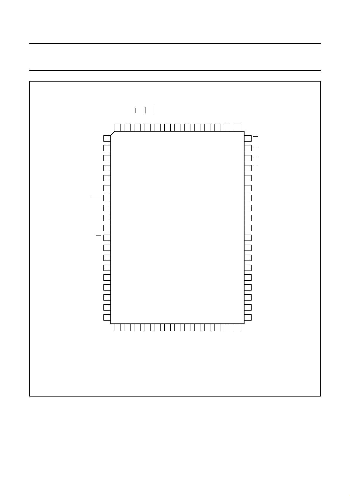
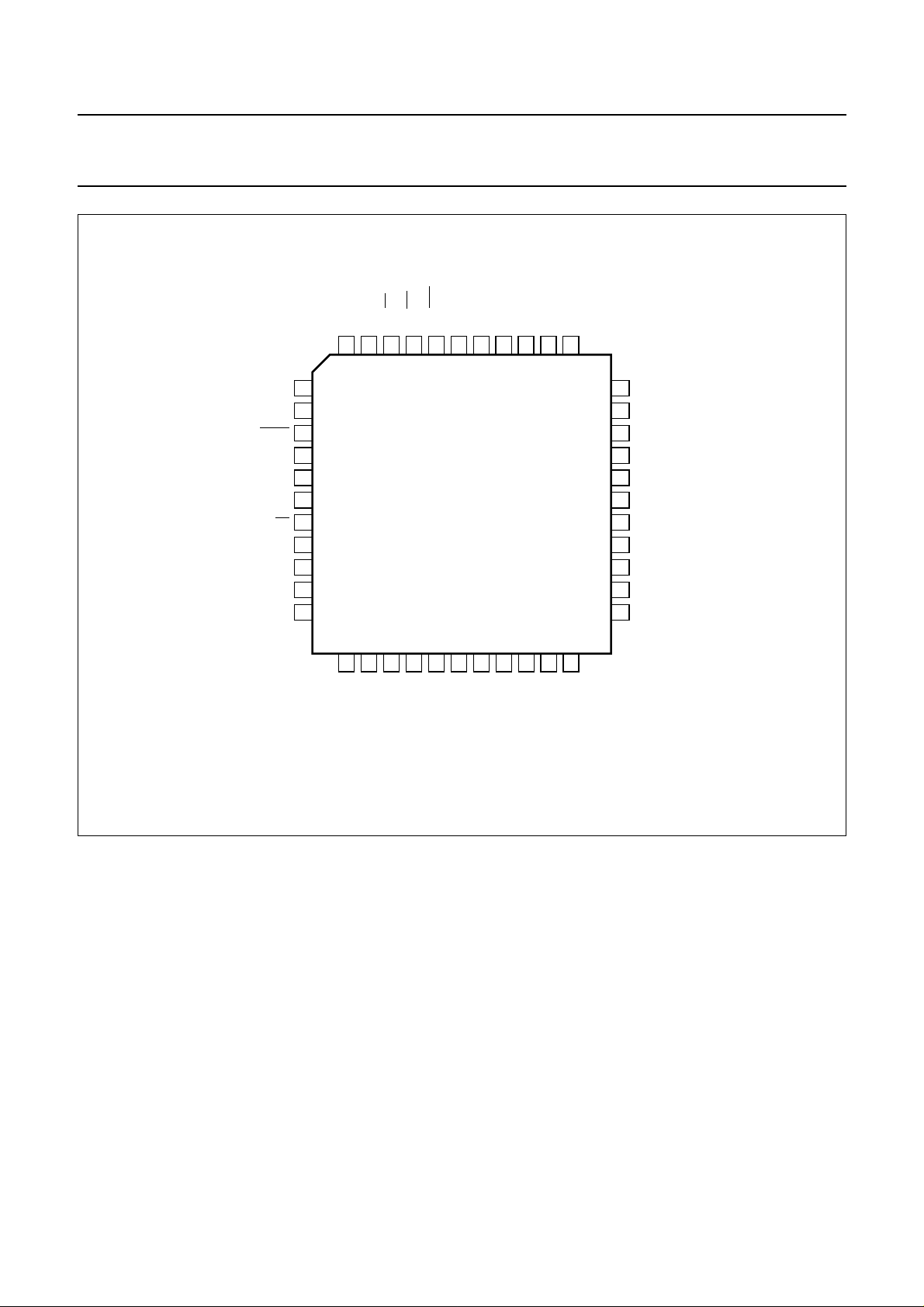
PINNING
SYMBOL
DESCRIPTION
QFP64 QFP44
P22 1 1 address 10/general purpose I/O port
P23 2 2 address 11/general purpose I/O port
P24 3 − address 12/general purpose I/O port
P25 4 − address 13/general purpose I/O port
P26 5 − address 14/general purpose I/O port
P27 6 − address 15/general purpose I/O port
PSEN 7 3 program store enable output
ALE 8 4 address latch enable
XTAL2 9 5 crystal connection
XTAL1 10 6 crystal connection or external clock input
EA 11 7 external access
P07 12 − address/data 7/general purpose I/O port
P06 13 − address/data 6/general purpose I/O port
P05 14 − address/data 5/general purpose I/O port
P04 15 − address/data 4/general purpose I/O port
P03 16 8 address/data 3/general purpose I/O port
P02 17 9 address/data 2/general purpose I/O port
P01 18 10 address/data 1/general purpose I/O port
P00 19 11 address/data 0/general purpose I/O port
n.c. 20 12 not connected
n.c. 21 13 not connected
n.c. 22 − not connected
PIN
V
DDRAM
23 14 supply voltage for the auxiliary RAM
GNDRAM 24 15 ground for the auxiliary RAM
n.c. 25 − not connected
RST 26 16 card reset output (ISO C2 contact)
CLK 27 17 clock output to the card (ISO C3 contact)
AGND 28 18 ground for the analog part
S1 29 19 contact 1 for the step-up converter (a ceramic capacitor of 100 nF must be
connected between S1 and S2)
V
DDA
30 20 analog supply voltage for the voltage doubler
S2 31 21 contact 2 for the step-up converter (a ceramic capacitor of 100 nF must be
connected between S1 and S2)
VUP 32 22 output of the step-up converter; must be decoupled with a 100 nF ceramic
capacitor
n.c. 33 − not connected
n.c. 34 − not connected
n.c. 35 − not connected
V
CC
36 23 card supply output voltage (ISO C1 contact)
1998 Jul 31 5
Philips Semiconductors Product specification
Multiprotocol IC Card coupler TDA8006
SYMBOL
I/O 37 24 data line to/from the card (ISO C7 contact)
C4 38 25 auxiliary I/O for ISO C4 contact (synchronous cards for instance)
C8 39 26 auxiliary I/O for ISO C8 contact (synchronous cards for instance)
GND 40 27 ground
V
DD
PRES 42 29 card presence contact input (active HIGH or LOW by mask option); see Table 12
CLKOUT 43 30 output for clocking external devices
CDELAY 44 31 external capacitor connection for delayed reset signal
ALARM 45 32 open drain reset output (active HIGH or LOW by mask option); see Table 12
TEST 46 33 test pin (must be left open-circuit in the application)
INHIB 47 − test pin (must be left open-circuit in the application)
K0 48 − output port from port extension (±2 mA push-pull)
K1 49 − output port from port extension (±2 mA push-pull)
K2 50 − output port from port extension (±2 mA push-pull)
K3 51 − output port from port extension (±2 mA push-pull)
RESET 52 34 input for resetting the microcontroller (active HIGH)
P10/T2 53 35 general purpose I/O port (connected to P10)
P11/T2EX 54 36 general purpose I/O port (connected to P11)
n.c. 55 37 not connected
n.c. 56 − not connected
n.c. 57 − not connected
P30/RXD 58 38 general purpose I/O port or serial interface receive line
P31/TXD 59 39 general purpose I/O port or serial interface transmit line
INT1 60 40 general purpose I/O port or interrupt (connected to P33)
P33/
P36/
WR 61 41 general purpose I/O port or external data memory write strobe
RD 62 42 general purpose I/O port or external data memory read strobe
P37/
P20 63 43 address 8/general purpose I/O port
P21 64 44 address 9/general purpose I/O port
QFP64 QFP44
PIN
DESCRIPTION
41 28 supply voltage
1998 Jul 31 6
Philips Semiconductors Product specification
Multiprotocol IC Card coupler TDA8006
handbook, full pagewidth
P22
P23
P24
P25
P26
P27
PSEN
ALE
XTAL2
XTAL1
EA
P07
P06
P05
P04
P03
P02
P01
P00
P21
64
1
2
3
4
5
6
7
8
9
10
11
12
13
14
15
16
17
18
19
P20
63
P37/RD
62
61
P36/WR
P33/INT1
60
P30/RXD
P31/TXD
59
58
TDA8006H
n.c.
57
n.c.
56
n.c.
55
P11/T2EX
P10/T2
54
53
RESET
52
51
50
49
48
47
46
45
44
43
42
41
40
39
38
37
36
35
34
33
K3
K2
K1
K0
INHIB
TEST
ALARM
CDELAY
CLKOUT
PRES
V
DD
GND
C8
C4
I/O
V
CC
n.c.
n.c.
n.c.
20
21
22
23
24
25
n.c.
n.c.
n.c.
DDRAM
V
n.c.
GNDRAM
Fig.2 Pin configuration (QFP64).
1998 Jul 31 7
26
RST
27
CLK
28
AGND
29
S1
30
DDA
V
31
S2
32
VUP
MGR226
Philips Semiconductors Product specification
Multiprotocol IC Card coupler TDA8006
handbook, full pagewidth
P20
P37/RD
P36/WR
P33/INT1
P31/TXD
P30/RXD
P11/T2EX
P10/T2
P21
44
n.c.
43
42
41
40
39
38
37
RESET
36
35
34
P22
P23
PSEN
ALE
XTAL2
XTAL1
EA
P03
P02
P01
P00
22
VUP
33
TEST
ALARM
32
31
CDELAY
30
CLKOUT
PRES
29
V
28
GND
27
C8
26
C4
25
24
I/O
V
23
MGR227
DD
CC
1
2
3
4
5
6
7
8
9
10
11
12
13
n.c.
n.c.
TDA8006AH
14
15
DDRAM
V
GNDRAM
16
RST
17
CLK
18
AGND
19
S1
20
DDA
V
21
S2
Fig.3 Pin configuration (QFP44).
1998 Jul 31 8

Philips Semiconductors Product specification
Multiprotocol IC Card coupler TDA8006
FUNCTIONAL DESCRIPTION
It is assumed that the reader of this data sheet is familiar
with ISO 7816.
Microcontroller
The microcontroller is an 80C52 with 16 kbytes of ROM,
256 bytes of RAM, timers 0, 1, 2 and 5 I/O ports (port P0:
open-drain; ports P1 to P3: weak pull-up). Port P4 is as in
83CE560, except that precharge circuitries ensure fast
rising time also when leaving read mode (transition times
<0.5 µs). The ROM code content may be tested by
signature, thus avoiding read-out of the ROM code after
masking (for security bit option see Table 12). The CPU,
timers 0 and 1, serial UART, parallel I/O ports, 256-byte
RAM, 16-kbyte ROM and external bus are conventional
C51 family library elements. Timer 2 is a conventional
C52 element (interrupt enable bit ET2: bit 3 in register
IEN1 at byte address E8H and interrupt priority bit PT2:
Table 1 List of differences between TDA8006, CE560, CL580 and C52
FEATURES TDA8006 83CE560 CL580 INTEL C52
P4 address C0 C0 C1 no
Timer 2 Intel Philips Intel Intel
ROM size 16 kbytes 64 kbytes 6 kbytes 8 kbytes
External 0 interrupt
vector
External 0 interrupt
priority
Timer 0 interrupt vector 000BH 000BH 000BH 000BH
Timer 0 interrupt priority 2nd 2nd 4th 2nd
External 1 interrupt
vector
External 1 interrupt
priority
Timer 1 interrupt vector 001BH 001BH 001BH 001BH
Timer 1 interrupt priority 4th 4th 10th 4th
Serial 0 interrupt vector 0023H 0023H 0023H 0023H
Serial 0 interrupt priority 5th 5th 13th 5th
Timer 2 interrupt vector 004BH 0033H, etc. (8) 0033H 002BH
Timer 2 interrupt priority lowest (6th) miscellaneous 5th lowest (6th)
2
I
C no yes yes no
ADC no yes yes no
32 kHz oscillator no yes no no
PWM no yes yes no
Watchdog no yes yes no
0003H 0003H 0003H 0003H
highest (1st) highest (1st) highest (1st) highest (1st)
0013H 0013H 0013H 0013H
3th 3th 7th 3th
bit 3 in register IP1 at byte address F8H). Register PCON
contains an added feature: PCON.5 = RFI (reduced radio
frequency interference bit). When set to logic 1, the
toggling of pin ALE is prohibited. This pin is cleared on
RESET.
If an access to the external data memory via MOVX
instructions (see Table 1) is desired, bit PCON.6 = ARD
inside the PCON register must be set to logic 1.
Please refer for any further information to the published
specification of the 83CE560 in
80C51-Based 8-Bit Microcontrollers”
Ports P40 to P47,INT0, P12, P13, P14, P15, P16 and P17
are used internally for controlling the smart card interface
and the other peripherals. P34 and P35 are used to control
the auxiliary contacts C4 and C8.
The list of differences given in Table 1 may help to develop
the software on the dedicated emulation board for
TDA8006 or other device.
“Data Handbook IC20;
.
1998 Jul 31 9
Philips Semiconductors Product specification
Multiprotocol IC Card coupler TDA8006
FEATURES TDA8006 83CE560 CL580 INTEL C52
Interrupts on P1 no no yes no
Additional RAM 1-kbyte peripheral 2-kbyte MOVX no no
Wake-up from PDOWN reset,
Table 2 Bit addresses (special function registers)
INT0, INT1 reset, INT0,
INT1 + other
reset, INT2 to INT8 reset
REGISTER
IP1 −−−−PT2 −−− XXXX 0XXX
B 0000 0000
IEN1 −−−−ET2 −−− 0000 0000
ACC 0000 0000
PSW CY AC F0 RS1 RS0 OV F1 P 0000 0000
T2CON TF2 EXF2 RCLK TCLK EXEN2 TR2 C/T2N CP/RL2N 0000 0000
P4 1111 1111
IP0 −−−PS0 PT1 PX1 PT0 PX0 XXX0 0000
P3 1111 1111
IEN0 EA −−ES0 ET1 EX1 ET0 EX0 0XX0 0000
P2 1111 1111
S0CON SMO SM1 SM2 REN TB8 RB8 TI RI 0000 0000
P1 1111 1111
TCON TF1 TR1 TF0 TR0 IE1 IT1 IE0 IT0 0000 0000
P0 1111 1111
BYTE
ADDRESS
F8H FFH FEH FDH FCH FBH FAH F9H F8H
F0H F7H F6H F5H F4H F3H F2H F1H F0H
E8H EFH EEH EDH ECH EBH EAH E9H E8H
E0H E7H E6H E5H E4H E3H E2H E1H E0H
D0H D7H D6H D5H D4H D3H D2H D1H D0H
C8H CFH CEH CDH CCH CBH CAH C9H C8H
C0H C7H C6H C5H C4H C3H C2H C1H C0H
B8H BFH BEH BDH BCH BBH BAH B9H B8H
B0H B7H B6H B5H B4H B3H B2H B1H B0H
A8H AFH AEH ADH ACH ABH AAH A9H A8H
A0H A7H A6H A5H A4H A3H A2H A1H A0H
98H 9FH 9EH 9DH 9CH 9BH 9AH 99H 98H
90H 97H 96H 95H 94H 93H 92H 91H 90H
88H 8FH 8EH 8DH 8CH 8BH 8AH 89H 88H
80H 87H 86H 85H 84H 83H 82H 81H 80H
(MSB) (LSB)
BIT ADDRESS
RESET
VALUE
1998 Jul 31 10
Philips Semiconductors Product specification
Multiprotocol IC Card coupler TDA8006
Table 3 Bit addresses (other registers)
REGISTER
BYTE
ADDRESS
RESET VALUE
SP 81H 0000 1111
DPL 82H 0000 0000
DPH 83H 0000 0000
PCON 87H 0000 0000
TMOD 89H 0000 0000
TL0 8AH 0000 0000
TL1 8BH 0000 0000
TH0 8CH 0000 0000
TH1 8DH 0000 0000
S0BUF 99H XXXX XXXX
RCAP2L CAH 0000 0000
RCAP2H CBH 0000 0000
TL2 CCH 0000 0000
TH2 CDH 0000 0000
Supply
The circuit operates within a supply voltage range of
4.2 to 6 V. The supply pins are VDD, V
V
and GNDRAM. Pins V
DDRAM
and AGND supply the
DDA
, GND, AGND,
DDA
analog drivers to the card and have to be externally
decoupled because of the large current spikes that the
card and the step-up converter can create. V
DDRAM
and
GNDRAM supply the auxiliary RAM and should be
decoupled separately. VDD and GND supply the rest of the
chip. An integrated spike killer ensures the contacts to the
card remain inactive during power-up or power-down.
An internal voltage reference is generated which is used
within the step-up converter, the voltage supervisor and
the V
generator.
CC
The voltage supervisor generates an alarm pulse, whose
length is defined by an external capacitor tied to the
CDELAY pin, when VDD is too low to ensure proper
operation (1 ms per 1 nF typical). This pulse is used as a
reset pulse by the controller, in parallel with an external
reset input, which can be tied to the system controller. It is
also used in order to either block any spurious on card
contacts during controllers reset or to force an automatic
deactivation of the contacts in the event of supply drop-out
(see Sections “Activation sequence” and “Deactivation
sequence”). It is also fed to an external open-drain output
(called ALARM) which can be chosen active HIGH or LOW
by mask option (see Table 12).
1998 Jul 31 11

Philips Semiconductors Product specification
Multiprotocol IC Card coupler TDA8006
handbook, full pagewidth
V
V
DD
CDELAY
ALARM
th(VDD)
V
th(CDELAY)
t
W
Fig.4 Voltage supervisor.
Step-up converter
Except for the VCC generator and the other card contacts
buffers, the whole circuit is powered by VDD, V
V
. If the supply voltage is 4.2 V, then a higher
DDRAM
DDA
and
voltage is needed for the ISO contacts supply. When a
card session is requested by the controller, the sequencer
first starts the step-up converter, which is a switched
capacitors type, clocked by an internal oscillator at a
frequency of approximately 2.5 MHz. The output voltage
VUP is regulated at approximately 6 V and then fed to the
generator. VCC and GND are used as a reference for
V
CC
all other cards contacts.
ISO 7816 security
The correct sequence during activation and deactivation of
the card is ensured through a specific sequencer, clocked
by a division ratio of the internal oscillator.
Activation (bit CMDVCC within the ports extension register
is HIGH) is only possible if the card is present (pin PRES
HIGH or LOW according to mask option) and if the supply
voltage is correct (ALARM signal inactive).
The presence of the card is signalled to the controller by
the OFF bit (within the status register, generating an
interrupt if enabled when toggling).
During a session, the sequencer performs an automatic
emergency deactivation in the event of card take-off,
supply voltage drop or short-circuit. The OFF bit goes
LOW, thereby warning the controller through the interrupt
line
INT0 and the status register.
MGR228
Peripheral interface (see Figs 5 and 6)
This block allows parallel communication with the four
peripherals (ISO 7816 UART, clock generator, on/off
sequencer and auxiliary RAM) through an 8-bit data bus,
6-bit address and control bus and one interrupt line to the
controller. The data bus consists of ports P40 (data 0) to
P47 (data 7). The address bus consists of ports AD0
(P12), AD1 (P13), AD2 (P14) and AD3 (P15). The control
lines are R/
W (P16) and EN (P17). The interrupt line is
INT0.
During a read operation, data is available on the bus when
EN is LOW and the controller may read them at this
moment. During a write operation, the data should be
present on the bus before assertingEN LOW, which writes
them in the registers. After resetting EN HIGH, the
controller must not omit to release the bus by setting P4
HIGH again (the transition times on port P4 are less than
500 ns).
The interrupt line is reset HIGH when reading out the
status register.
EAD OPERATION
R
• Set P4 to FFH
• Select the register with AD0, AD1, AD2, AD3
• Assert R/W HIGH
• Assert EN LOW; the data is available on data bus P4
• Read the data on P4
• Set EN HIGH: the bus is set to high impedance.
1998 Jul 31 12
 Loading...