

Philips TDA8005H-C127, TDA8005H-C122, TDA8005H-C107, TDA8005G-C107, TDA8005G-C119 Datasheet
...
DATA SH EET
Product specification
Supersedes data of 1995 Apr 13
File under Integrated Circuits, IC17
1996 Sep 25
INTEGRATED CIRCUITS
TDA8005
Low-power smart card coupler

1996 Sep 25 2
Philips Semiconductors Product specification
Low-power smart card coupler TDA8005
FEATURES
• VCC generation (5 V ±5%, 20 mA maximum with
controlled rise and fall times)
• Clock generation (up to 8 MHz), with two times
synchronous frequency doubling
• Clock STOP HIGH, clock STOP LOW or 1.25 MHz (from
internal oscillator) for cards power-down mode
• Specific UART on I/O for automatic direct/inverse
convention settings and error management at
character level
• Automatic activation and deactivation sequences
through an independent sequencer
• Supports the protocol T = 0 in accordance with
ISO 7816, GSM11.11 requirements (Global System for
Mobile communication); and EMV banking specification
approved for Final GSM11.11 Test Approval (FTA)
• Several analog options are available for different
applications (doubler or tripler DC/DC converter, card
presence, active HIGH or LOW, threshold voltage
supervisor, etc.
• Overloads and take-off protections
• Current limitations in the event of short-circuit
• Special circuitry for killing spikes during power-on or off
• Supply supervisor
• Step-up converter (supply voltage from 2.5 to 6 V)
• Power-down and sleep mode for low-power
consumption
• Enhanced ESD protections on card side
(6 kV minimum)
• Control and communication through a standard RS232
full duplex interface
• Optional additional I/O ports for:
– keyboard
– LEDs
– display
– etc.
• 80CL51 microcontroller core with 4 kbytes ROM and
256-byte RAM.
APPLICATIONS
• Portable smart card readers for protocol T = 0
• GSM mobile phones.
GENERAL DESCRIPTION
The TDA8005 is a low cost card interface for portable
smart card readers. Controlled through a standard serial
interface, it takes care of all ISO 7816 and GSM11-11
requirements. It gives the card and the set a very high level
of security, due to its special hardware against ESD,
short-circuiting, power failure, etc. Its integrated step-up
converter allows operation within a supply voltage range of
2.5 to 6 V.
The very low-power consumption in Power-down and
sleep modes saves battery power. A special version where
the internal connections to the controller are fed outside
through pins allows easy development and evaluation,
together with a standard 80CL51 microcontroller.
Development tools, application report and support
(hardware and software) are available.
The device can be supplied either as a masked chip with
standard software handling all communication between
smart card and a master controller in order to make the
application easier, or as a maskable device.
1996 Sep 25 3
Philips Semiconductors Product specification
Low-power smart card coupler TDA8005
QUICK REFERENCE DATA
ORDERING INFORMATION
SYMBOL PARAMETER CONDITIONS MIN. TYP. MAX. UNIT
V
DD
supply voltage doubler and tripler option 2.5 − 6.0 V
I
DD(pd)
supply current in power-down mode VDD= 5 V; card inactive −−100 µA
I
DD(sm)
supply current in sleep mode doubler card powered but clock
stopped
−−500 µA
I
DD(sm)
supply current in sleep mode tripler card powered but clock
stopped
−−500 µA
I
DD(om)
supply current in operating mode unloaded; f
xtal
= 13 MHz;
f
µC
= 6.5 MHz;
f
card
= 3.25 MHz
−−5.5 mA
V
CC
card supply voltage including static and
dynamic loads on 100 nF
capacitor
4.75 5.0 5.25 V
I
CC
card supply current operating −−20 mA
limitation −−30 mA
SR slew rate on V
CC
(rise and fall) maximum load capacitor
150 nF (including typical
100 nF decoupling)
0.05 0.1 0.15 V/µs
t
de
deactivation cycle duration −−100 µs
t
act
activation cycle duration −−100 µs
f
xtal
crystal frequency 2 − 16 MHz
T
amb
operating ambient temperature −25 − +85 °C
TYPE
NUMBER
PACKAGE
NAME DESCRIPTION VERSION
TDA8005G LQFP64 plastic low profile quad flat package; 64 leads; body 10 × 10 × 1.4 mm SOT314-2
TDA8005H QFP44 plastic quad flat package; 44 leads (lead length 1.3 mm);
body 10 × 10 × 1.75 mm
SOT307-2

1996 Sep 25 4
Philips Semiconductors Product specification
Low-power smart card coupler TDA8005
BLOCK DIAGRAM
Fig.1 Block diagram (LQFP64; SOT314-2).
handbook, full pagewidth
VOLTAGE SENSE
2.3 to 2.7 V
INTERNAL OSCILLATOR
2.5 MHz
TDA8005G
INTERNAL
REFERENCE
SUPPLY
ALARM
DELAY
RESET
AUX1
AUX2
INT1
XTAL1 XTAL2
DGND AGND
P00
to
P37
RxD
TxD
OPTIONAL
PORTS
PERIPHERAL
INTERFACE
CONTROLLER
CL51
ISO 7816 UART
CLOCK CIRCUITRY
OUTPUT PORT
EXTENSION
STEP-UP CONVERTER
4 kbytes ROM
256-byte RAM
SECURITY
V
CC
GENERATOR
RST
BUFFER
I/O
BUFFER
CLOCK
BUFFER
SEQUENCER
S1 S2
47 nF
100 nF
100 nF
S3 S4
47 nF
V
DDD
V
DDA
2.5 to 6 V
63
10
44
46
22
28
29
32
33
30
(1)
36 35 37 2 53
K0 K1 K2 K3 K4 K5
52 51 50 49
47
57
55
56
58
59
4
UP S5
V
60
47 nF
LIS
V
CC
100 nF
RST
I/O
CLK
PRES
EN1
EN2
EN3
EN4
start
RST
off
64 61 3 62
alarm
V
DDD
skill
data clk EN S0 S1 R/W
µCclk
I/O
INT
ref
V
DDD
osc ref
osc
MLD210
(1) For details see Chapter “Pinning”.

1996 Sep 25 5
Philips Semiconductors Product specification
Low-power smart card coupler TDA8005
PINNING
SYMBOL
PIN
DESCRIPTION
LQFP64
SOT314-2
QFP44
SOT307-2
n.c. 1 − not connected
AGND 2 1 analog ground
S3 3 2 contact 3 for the step-up converter
K5 4 − output port from port extension
P03 5 3 general purpose I/O port (connected to P03)
P02 6 4 general purpose I/O port (connected to P02)
P01 7 5 general purpose I/O port (connected to P01)
n.c. 8 − not connected
P00 9 6 general purpose I/O port (connected to P00)
V
DDD
10 7 digital supply voltage
n.c. 11 − not connected
TEST1 12 8 test pin 1 (connected to P10; must be left open-circuit in the application)
P11 13 9 general purpose I/O port or interrupt (connected to P11)
P12 14 10 general purpose I/O port or interrupt (connected to P12)
P13 15 11 general purpose I/O port or interrupt (connected to P13)
P14 16 12 general purpose I/O port or interrupt (connected to P14)
n.c. 17 − not connected
P15 18 13 general purpose I/O port or interrupt (connected to P15)
P16 19 14 general purpose I/O port or interrupt (connected to P16)
TEST2 20 15 test pin 2 (connected to PSEN; must be left open-circuit in the application)
P17 21 16 general purpose I/O port or interrupt (connected to P17)
RESET 22 17 input for resetting the microcontroller (active HIGH)
n.c. 23 − not connected
n.c. 24 − not connected
n.c. 25 − not connected
n.c. 26 − not connected
n.c. 27 − not connected
RxD 28 18 serial interface receive line
TxD 29 19 serial interface transmit line
INT1 30 20 general purpose I/O port or interrupt (connected to P33)
T0 31 21 general purpose I/O port (connected to P34)
AUX1 32 22 push-pull auxiliary output (±5 mA; connected to timer T1 e.g. P35)
AUX2 33 23 push-pull auxiliary output (±5 mA; connected to timer P36)
P37 34 24 general purpose I/O port (connected to P37)
XTAL2 35 25 crystal connection
XTAL1 36 26 crystal connection or external clock input
DGND 37 27 digital ground
n.c. 38 − not connected
1996 Sep 25 6
Philips Semiconductors Product specification
Low-power smart card coupler TDA8005
n.c. 39 − not connected
P20 40 28 general purpose I/O port (connected to P20)
P21 41 − general purpose I/O port (connected to P21)
P22 42 29 general purpose I/O port (connected to P22)
P23 43 30 general purpose I/O port (connected to P23)
ALARM 44 − open-drain output for Power-On Reset (active HIGH or LOW by mask option)
n.c. 45 − not connected
DELAY 46 31 external capacitor connection for delayed reset signal
PRES 47 32 card presence contact input (active HIGH or LOW by mask option)
TEST3 48 33 test pin 3 (must be left open-circuit in the application)
K4 49 − output port from port extension
K3 50 − output port from port extension
K2 51 − output port from port extension
K1 52 − output port from port extension
K0 53 − output port from port extension
TEST4 54 34 test pin 4 (must be left open-circuit in the application)
I/O 55 35 data line to/from the card (ISO C7 contact)
RST 56 36 card reset output (ISO C2 contact)
CLK 57 37 clock output to the card (ISO C3 contact)
V
CC
58 38 card supply output voltage (ISO C1 contact)
LIS 59 39 supply for low-impedance on cards contacts
S5 60 40 contact 5 for the step-up converter
S2 61 41 contact 2 for the step-up converter
S4 62 42 contact 4 for the step-up converter
V
DDA
63 43 analog supply voltage
S1 64 44 contact 1 for the step-up converter
SYMBOL
PIN
DESCRIPTION
LQFP64
SOT314-2
QFP44
SOT307-2
1996 Sep 25 7
Philips Semiconductors Product specification
Low-power smart card coupler TDA8005
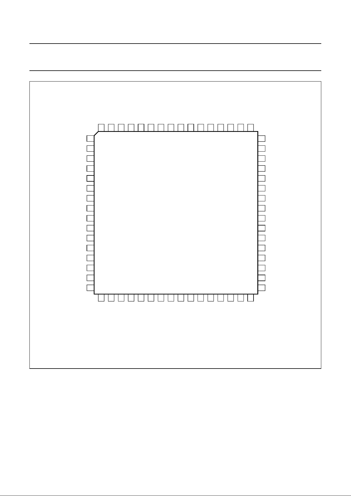
Fig.2 Pin configuration (LQFP64; SOT314-2).
handbook, full pagewidth
TDA8005G
MLD211
1
2
3
4
5
6
7
8
9
10
11
12
13
14
15
16
48
47
46
45
44
43
42
41
40
39
38
37
36
35
34
33
17
18
19
20
21
22
23
24
25
26
27
28
29
30
31
32
64
63
62
61
60
59
58
57
56
55
54
53
52
51
50
49
n.c.
P14
AGND
S3
K5
P03
P02
P01
n.c.
P00
V
n.c.
TEST1
P11
P12
P13
DDD
n.c.
AUX1
P15
P16
TEST2
P17
RESET
n.c.
n.c.
n.c.
n.c.
RxD
TxD
INT1
T0
n.c.
TEST3
PRES
DELAY
n.c.
ALARM
P23
P22
P21
P20
n.c.
n.c.
DGND
XTAL1
XTAL2
P37
AUX2
VS1S4
S2
S5.
LIS
V
CLK
RST
I/O
TEST4K0K1
K2
K3
K4
DDA
CC

1996 Sep 25 8
Philips Semiconductors Product specification
Low-power smart card coupler TDA8005
Fig.3 Pin configuration (QFP44; SOT307-2).
handbook, full pagewidth
TDA8005H
MLD212
1
2
3
4
5
6
7
8
9
10
11
33
32
31
30
29
28
27
26
25
24
23
12
13
14
15
16
17
18
19
20
21
22
44
43
42
41
40
39
38
37
36
35
34
AGND
S3
P03
P02
P01
P00
DDD
TEST1
P11
P12
P13
V
P14
P15
P16
TEST2
P17
RESET
RxD
TxD
INT1
T0
AUX1
TEST3
PRES
DELAY
P23
P22
P20
DGND
XTAL1
XTAL2
P37
AUX2
S1
V
S4
S2
S5
LIS
V
CLK
RST
I/O
TEST4
DDA
CC
1996 Sep 25 9
Philips Semiconductors Product specification
Low-power smart card coupler TDA8005
FUNCTIONAL DESCRIPTION
Microcontroller
The microcontroller is an 80CL51 with 256 bytes of RAM
instead of 128. The baud rate of the UART has been
multiplied by four in modes 1, 2 and 3 (which means that
the division factor of 32 in the formula is replaced by 8 in
both reception and transmission, and that in the reception
modes, only four samples per bit are taken with decision
on the majority of samples 2, 3 and 4) and the delay
counter has been reduced from 1536 to 24.
Remark: this has an impact when getting out of
PDOWN mode. It is recommended to switch to internal
clock before entering PDOWN mode
(see
“application report”
).
All the other functions remain unchanged. Please, refer to
the published specification of the 80CL51 for any further
information. Pins INT0, P10, P04 to P07 and P24 to P27
are used internally for controlling the smart card interface.
Mode 0 is unchanged. The baud rate for modes 1 and 3 is:
The baud rate for mode 2 is:
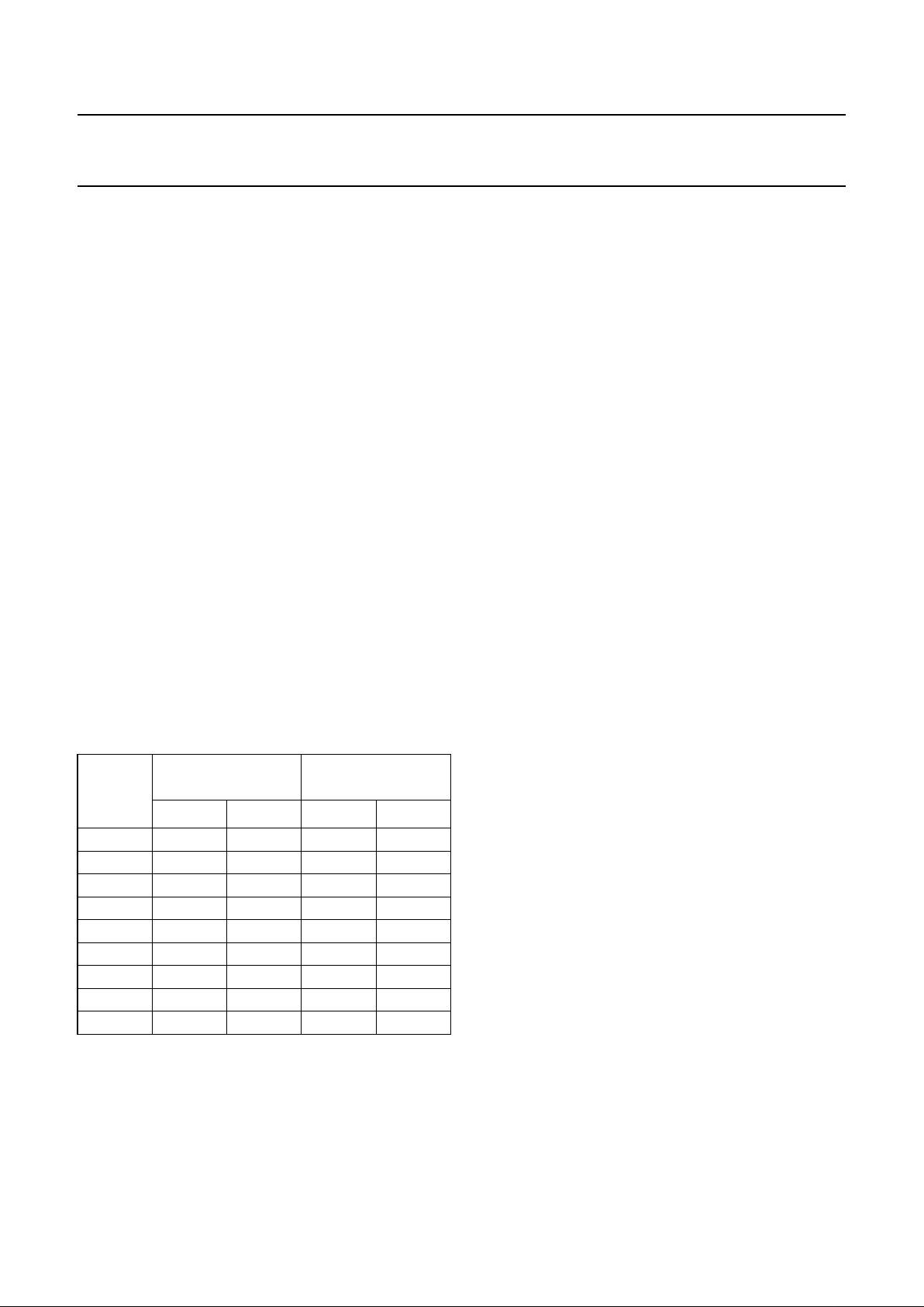
Table 1 Mode 3 timing
BAUD
RATE
f
clk
= 6.5 MHz;
VDD=5V
f
clk
= 3.25 MHz;
VDD=5or3V
SMOD TH1 SMOD TH1
135416 1 255 −−
67708 0 255 1 255
45139 1 253 −−
33854 0 254 0 255
27083 1 251 −−
22569 0 253 1 253
16927 −−0 254
13542 −−1 251
11285 0 250 0 253
2
SMOD
8
----------------- -
f
clk
12 256 TH1 )–(×
--------------------------------------------------
×
2
SMOD
16
----------------- -
f
clk
×
Supply
The circuit operates within a supply voltage range of
2.5 to 6 V. The supply pins are V
DDD
, DGND and AGND.
Pins V
DDA
and AGND supply the analog drivers to the card
and have to be externally decoupled because of the large
current spikes that the card and the step-up converter can
create. An integrated spike killer ensures the contacts to
the card remain inactive during power-up or power-down.
An internal voltage reference is generated which is used
within the step-up converter, the voltage supervisor, and
the V
CC
generator.
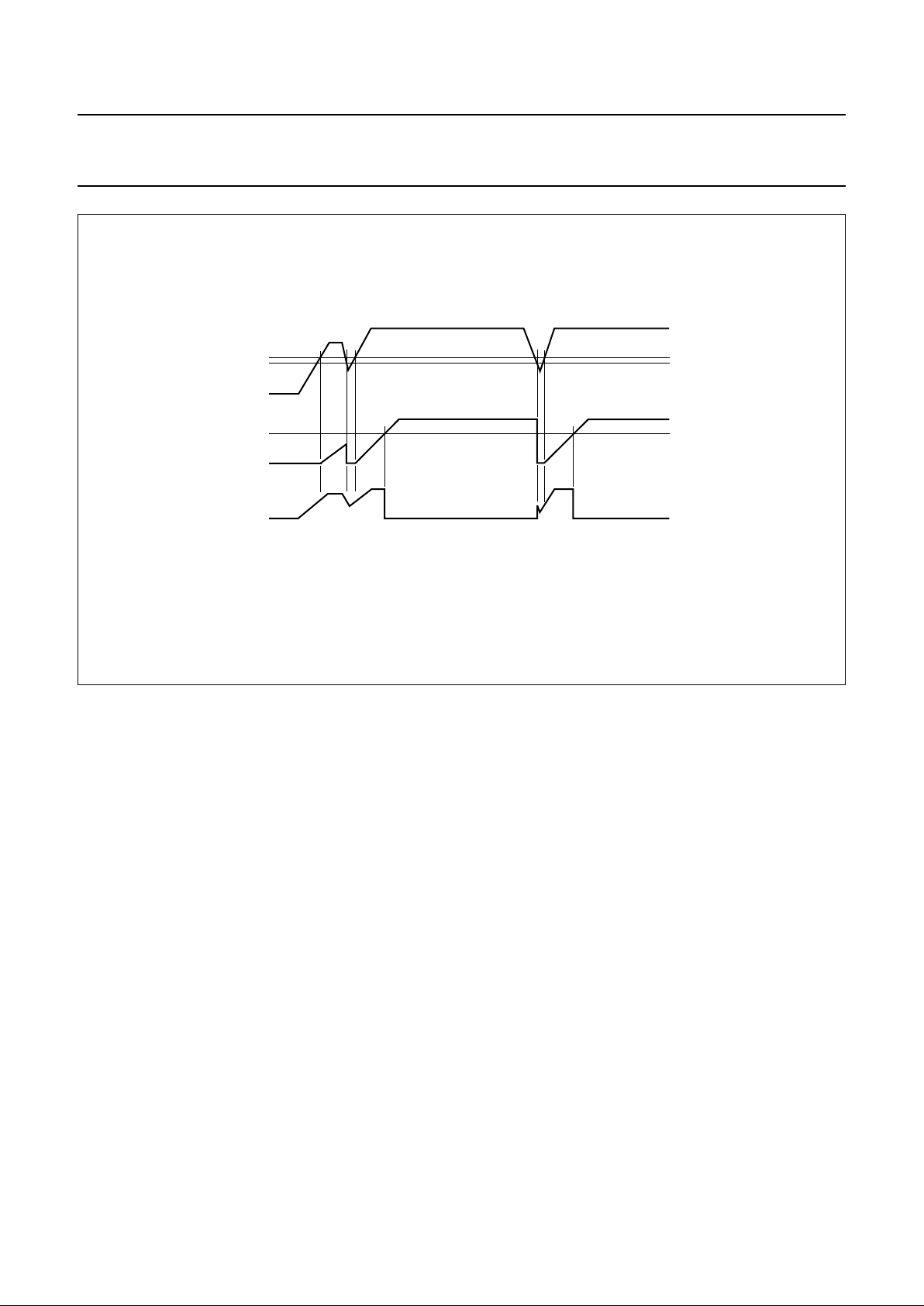
The voltage supervisor generates an alarm pulse, whose
length is defined by an external capacitor tied to the
DELAY pin, when V
DDD
is too low to ensure proper
operation (1 ms per 1 nF typical). This pulse is used as a
RESET pulse by the controller, in parallel with an external
RESET input, which can be tied to the system controller.
It is also used in order to either block any spurious card
contacts during controllers reset, or to force an automatic
deactivation of the contacts in the event of supply drop-out
[see Sections “Activation sequence” and “Deactivation
sequence (see Fig.10)”].
In the 64 pin version, this reset pulse is output to the open
drain ALARM pin, which may be selected active HIGH or
active LOW by mask option and may be used as a reset
pulse for other devices within the application.
1996 Sep 25 10
Philips Semiconductors Product specification
Low-power smart card coupler TDA8005
Fig.4 Supply supervisor.
handbook, full pagewidth
MBH634
V
th1
+ V
hys1
V
th1
V
DD
V
th2
V
DEL
ALARM
Low impedance supply (pin LIS)
For some applications, it is mandatory that the contacts to
the card (VCC, RST, CLK and I/O) are low impedance while
the card is inactive and also when the coupler is not
powered. An auxiliary supply voltage on pin LIS ensures
this condition where I
LIS
=<5µA for V
LIS
= 5 V. This low
impedance situation is disabled when VCC starts rising
during activation, and re-enabled when the step-up
converter is stopped during deactivation. If this feature is
not required, the LIS pin must be tied to VDD.
Step-up converter
Except for the V
CC
generator, and the other cards contacts
buffers, the whole circuit is powered by V
DDD
and V
DDA
.
If the supply voltage is 3 V or 5 V, then a higher voltage is
needed for the ISO contacts supply. When a card session
is requested by the controller, the sequencer first starts the
step-up converter, which is a switched capacitors type,
clocked by an internal oscillator at a frequency
approximately 2.5 MHz. The output voltage, VUP, is
regulated at approximately 6,5 V and then fed to the V
CC
generator. VCC and GND are used as a reference for all
other cards contacts. The step-up converter may be
chosen as a doubler or a tripler by mask option, depending
on the voltage and the current needed on the card.
ISO 7816 security
The correct sequence during activation and deactivation of
the card is ensured through a specific sequencer, clocked
by a division ratio of the internal oscillator.
Activation (START signal P05) is only possible if the card
is present (PRES HIGH or LOW according to mask
option), and if the supply voltage is correct (ALARM signal
inactive), CLK and RST are controlled by RSTIN (P04),
allowing the correct count of CLK pulses during
Answer-to-Reset from the card.
The presence of the card is signalled to the controller by
the OFF signal (P10).
During a session, the sequencer performs an automatic
emergency deactivation in the event of card take-off,
supply voltage drop, or hardware problems. The OFF
signal falls thereby warning the controller.
 Loading...