

Philips TDA8004T-C1 Datasheet

DATA SH EET
Product specification
Supersedes data of 1997 Nov 21
File under Integrated Circuits, IC02
1999 Dec 30
INTEGRATED CIRCUITS
TDA8004T
IC card interface

1999 Dec 30 2
Philips Semiconductors Product specification
IC card interface TDA8004T
FEATURES
• 3 or 5 V supply for the IC (GND and VDD)
• Step-up converter for VCC generation (separately
powered with a 5 V ±10% supply, V
DDP
and PGND)
• 3 specific protected half duplex bidirectional buffered
I/O lines (C4, C7 and C8)
• VCC regulation 5 V ±5% on 2 × 100 nF or 1 × 100 nF
and 1 × 220 nF multilayer ceramic capacitors with low
ESR, ICC< 65 mA at 4.5 V < V
DDP
< 6.5 V, current
spikes of 40 nAs up to 20 MHz, withcontrolled rise and
fall times, filtered overload detection approximately
90 mA)
• Thermal and short-circuit protections on all card
contacts
• Automatic activation and deactivation sequences
(initiated by software or by hardware in the event of a
short-circuit, card take-off, overheating or supply
drop-out)
• Enhanced ESD protection on card side (>6 kV)
• 26 MHz integrated crystal oscillator
• Clock generation for the card up to 20 MHz (divided by
1, 2, 4 or 8 through CLKDIV1 and CLKDIV2 signals)
• Non-inverted control of RST via pin RSTIN
• ISO 7816, GSM11.11 and EMV (payment systems)
compatibility
• Supply supervisor for spikes killing during power-on and
power-off
• One multiplexed status signal OFF.
APPLICATIONS
• IC card readers for banking
• Electronic payment
• Identification
• Pay TV.
GENERAL DESCRIPTION
The TDA8004T is a complete low cost analog interface for
asynchronous smart cards. It can be placed betw the card
andthe microcontroller with very few external components
to perform all supply protection and control functions.
ORDERING INFORMATION
TYPE
NUMBER
PACKAGE
NAME DESCRIPTION VERSION
TDA8004T SO28 plastic small outline package; 28 leads; body width 7.5 mm SOT136-1
1999 Dec 30 3
Philips Semiconductors Product specification
IC card interface TDA8004T
QUICK REFERENCE DATA
SYMBOL PARAMETER CONDITIONS MIN. TYP. MAX. UNIT
Supplies
V
DD
supply voltage 2.7 − 6.5 V
V
DDP
step-up supply voltage 4.5 5 6.5 V
I
DD
supply current inactive mode; VDD= 3.3 V;
f
XTAL
=10MHz
−−1.2 mA
active mode; V
DD
= 3.3 V;
f
XTAL
= 10 MHz; no load
−−1.5 mA
I
DDP
step-up supply current inactive mode; V
DDP
=5V;
f
XTAL
=10MHz
−−0.1 mA
active mode; V
DDP
=5V;
f
XTAL
= 10 MHz; no load
−−18 mA
Card supply
V
CC
card supply voltage including
ripple
DC ICC < 65 mA 4.75 − 5.25 V
AC current spikes of 40 nAs 4.65 − 5.25 V
V
i(ripple)(p-p)
ripple voltage on V
CC
(peak-to-peak value)
20 kHz ≤f 200 MHz −−350 mV
I
CC
card supply current VCC from 0 to 5 V −−65 mA
General
f
CLK
card clock frequency 0 − 20 MHz
t
de
deactivation cycle duration 60 80 100 µs
P
tot
continuous total power dissipation T
amb
= −25 to +85 °C −−0.56 W
T
amb
ambient temperature −25 − +85 °C
1999 Dec 30 4
Philips Semiconductors Product specification
IC card interface TDA8004T
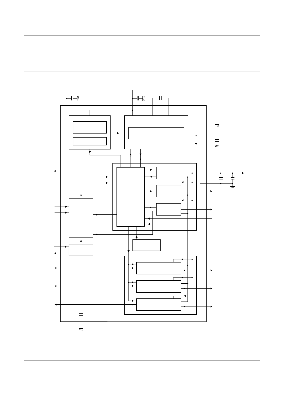
BLOCK DIAGRAM
handbook, full pagewidth
MGM175
100 nF
100 nF
100 nF
100 nF
100
nF
100
nF
I/O
TRANSCEIVER
I/O
TRANSCEIVER
I/O
TRANSCEIVER
THERMAL
PROTECTION
V
CC
GENERATOR
RST
BUFFER
CLOCK
BUFFER
SEQUENCER
CLOCK
CIRCUITRY
OSCILLATOR
HORSEQ
INTERNAL OSCILLATOR
2.5 MHz
STEP-UP CONVERTER
INTERNAL
REFERENCE
VOLTAGE SENSE
SUPPLY
EN2
PV
CC
EN5
EN4
EN3
CLK
EN1 CLKUP
ALARM
V
ref
21
V
DD
6
V
DDP
75
S1 S2
8
VUP
4
PGND
17
V
CC
16
14
RST
CGND
PRES
10
9
PRES
15
CLK
13
12
11
AUX1
AUX2
I/O
22
18
n.c.
GND
26
28
27
I/OUC
AUX2UC
AUX1UC
25
24
2
1
3
19
20
23
XTAL2
XTAL1
CLKDIV2
CLKDIV1
RFU1
CMDVCC
RSTIN
OFF
TDA8004T
Fig.1 Block diagram.
All capacitors are mandatory.
1999 Dec 30 5
Philips Semiconductors Product specification
IC card interface TDA8004T
PINNING
SYMBOL PIN I/O DESCRIPTION
CLKDIV1 1 I control with CLKDIV2 for choosing CLK frequency
CLKDIV2 2 I control with CLKDIV1 for choosing CLK frequency
RFU1 3 I reserved for future use (to be connected to V
DD
or microcontroller I/O; active HIGH)
PGND 4 supply power ground for step-up converter
S2 5 I/O capacitance connection for step-up converter (a 100 nF capacitor with ESR < 100 mΩ
must be connected between pins S1 and S2)
V
DDP
6 supply power supply voltage for step-up converter
S1 7 I/O capacitance connection for step-up converter (a 100 nF capacitor with ESR < 100 mΩ
must be connected between pins S1 and S2)
VUP 8 I/O output of step-up converter (a 100 nF capacitor with ESR < 100 mΩ must be
connected to PGND)
PRES 9 I card presence contact input (active LOW); if PRES orPRES is true, then the card is
considered as present
PRES 10 I card presence contact input (active HIGH); if PRES or
PRES is true, then the card is
considered as present
I/O 11 I/O data line to and from card (C7) (internal 10 kΩ pull-up resistor connected to V
CC
)
AUX2 12 I/O auxiliary line to and from card (C8) (internal 10 kΩ pull-up resistor connected to V
CC
)
AUX1 13 I/O auxiliary line to and from card (C4) (internal 10 kΩ pull-up resistor connected to V
CC
)
CGND 14 supply ground for card signals
CLK 15 O clock to card (C3)
RST 16 O card reset (C2)
V
CC
17 O Supply for card (C1); decouple to CGND with 2 × 100 nF or 1 × 100 nF and 1 × 220 nF
capacitors with ESR < 100 mΩ (with 220 nF, the noise margin on VCC will be higher).
n.c. 18 − not connected
CMDVCC 19 I start activation sequence input from microcontroller (active LOW)
RSTIN 20 I card reset input from microcontroller (active HIGH)
V
DD
21 supply supply voltage
GND 22 supply ground
OFF 23 O NMOS interrupt to microcontroller (active LOW) with 20 kΩ internal pull-up resistor
connected to VDD (refer section “Fault detection”)
XTAL1 24 I crystal connection or input for external clock
XTAL2 25 O crystal connection (leave open if an external clock source is used)
I/OUC 26 I/O microcontroller data I/O line (internal 10 kΩ pull-up resistor connected to V
DD
)
AUX1UC 27 I/O auxiliary line to and from microcontroller (internal 10 kΩ pull-up resistor connected to
V
DD
)
AUX2UC 28 I/O auxiliary line to and from microcontroller (internal 10 kΩ pull-up resistor connected to
V
DD
)
1999 Dec 30 6
Philips Semiconductors Product specification
IC card interface TDA8004T
FUNCTIONAL DESCRIPTION
Throughout this document, it is assumed that the reader is
familiar with ISO 7816 norm terminology.
Power supply
The supply pins for the IC are VDD and GND. VDD should
be in the range from 2.7 to 6.5 V. All interface signals with
the system controller are referenced to VDD; so, be sure
the supply voltage of the system controller is also VDD. All
card contacts remain inactive during powering up or
powering down. The sequencer is not activated until V
DD
reaches V
th2+Vhys(th2)
(see Fig.3). When VDDfalls below
V
th2
, an automatic deactivation of the contacts is
performed.
For generating a 5 V ±5% VCC supply to the card, an
integrated voltage doubler is incorporated. This step-up
converter should be separately supplied by V
DDP
and
PGND (from 4.5 to 6.5 V). Due to large transient currents,
the 2 × 100 nF capacitors of the step-up converter should
have an ESR less than 100 mΩ and be located as near as
possible to the IC.
The supply voltages VDD and V
DDP
may be applied to
the IC in any time sequence.
If a voltage between 7 and 9 V is available within the
application, this voltage may be tied to pin VUP, thus
blocking the step-up converter. In this case, V
DDP
must be
tiedtoVDDandthecapacitorbetweenpinsS1 and S2may
be omitted.
Voltage supervisor
This block surveys the VDD supply. A defined reset pulse
of approximately 10 ms (tW) is used internally for
maintainingthe IC in the inactive modeduringpoweringup
or powering down of VDD (see Fig.3).
As long as VDD is less than V
th2+Vhys(th2)
, the IC will
remaininactivewhateverthelevelsonthecommandlines.
This also lasts for the duration of tWafter VDDhas reached
a level higher than V
th2+Vhys(th2)
.
The system controller should not try to start an activation
during this time.
When VDDfalls below V
th2
, a deactivation sequence of the
contacts is performed.
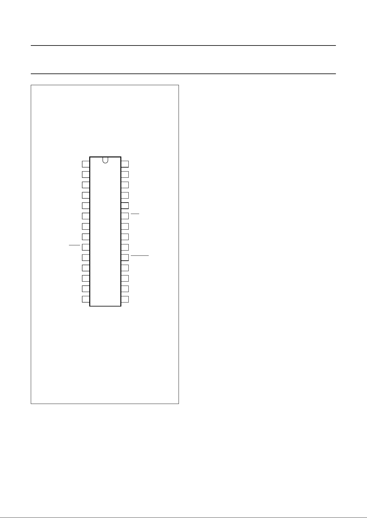
handbook, halfpage
CLKDIV1
CLKDIV2
RFU1
PGND
S2
V
DDP
S1
VUP
PRES
PRES
I/O
AUX2
AUX1
CGND
AUX2UC
AUX1UC
I/OUC
XTAL2
OFF
GND
XTAL1
V
DD
RSTIN
CMDVCC
n.c.
V
CC
RST
CLK
1
2
3
4
5
6
7
8
9
10
11
12
13
28
27
26
25
24
23
22
21
20
19
18
17
16
1514
TDA8004T
MGM174
Fig.2 Pin configuration.

1999 Dec 30 7
Philips Semiconductors Product specification
IC card interface TDA8004T
handbook, full pagewidth
MGM176
V
DD
t
W
t
W
V
th2
+ V
hys(th2)
V
th2
ALARM
(internal signal)
Fig.3 ALARM as a function of VDD (tW= 10 ms).
Clock circuitry
The clock signal (CLK) to the card is either derived from a
clock signal input on pin XTAL1 or from a crystal up to
26 MHz connected between pins XTAL1 and XTAL2.
The frequency may be chosen at
f
XTAL
,1⁄2f
XTAL
,1⁄4f
XTAL
or1⁄8f
XTAL
via pins CLKDIV1 and
CLKDIV2.
The frequency change is synchronous, which means that
during transition, no pulse is shorter than 45% of the
smallest period and that the first and last clock pulse
around the change has the correct width.
In the case of f
XTAL
, the duty factors are dependent on the
signal at XTAL1.
In order to reach a 45% to 55% duty factor on pin CLK the
input signal on XTAL1 should have a duty factor of
48% to 52% and transition times of less than 5% of the
input signal period.
If a crystal is used with f
XTAL
, the duty factor on pin CLK
may be 45% to 55% depending on the layout and on the
crystal characteristics and frequency.
Intheothercases,itisguaranteedbetween45% and 55%
of the period.
Thecrystaloscillatorrunsassoon as the IC is powered up.
If the crystal oscillator is used, or if the clock pulse on
XTAL1 is permanent, then the clock pulse will be applied
to the card according to the timing diagram of the
activation sequence (see Fig.5).
If the signal applied to XTAL1 is controlled by the system
controller, then the clock pulse will be applied to the card
when the system controller will send it (after completion of
the activation sequence).
Table 1 Clock circuitry definition
CLKDIV1 CLKDIV2 CLK
00
1
⁄
8
f
XTAL
01
1
⁄
4
f
XTAL
11
1
⁄
2
f
XTAL
10f
XTAL
1999 Dec 30 8
Philips Semiconductors Product specification
IC card interface TDA8004T
I/O circuitry
The three data lines I/O, AUX1 and AUX2 are identical.
The Idle state is realized by both lines (I/O and I/OUC)
being pulled HIGH via a 10 kΩ resistor (I/O to VCC and
I/OUC to VDD).
I/O is referenced to VCC and I/OUC to VDD, thus allowing
operation with VCC≠ VDD.
The first side on which a falling edge occurs becomes the
master.Ananti-latchcircuitdisablesthe detection of falling
edges on the other line, which becomes a slave.
After a time delay t
d(edge)
(approximately 200 ns), the
N transistor on the slave side is turned on, thus
transmitting the logic 0 present on the master side.
Whenthemastersidereturnstologic 1, the P transistor on
theslavesideisturnedon during the time delayt
d(edge)
and
then both sides return to their Idle states.
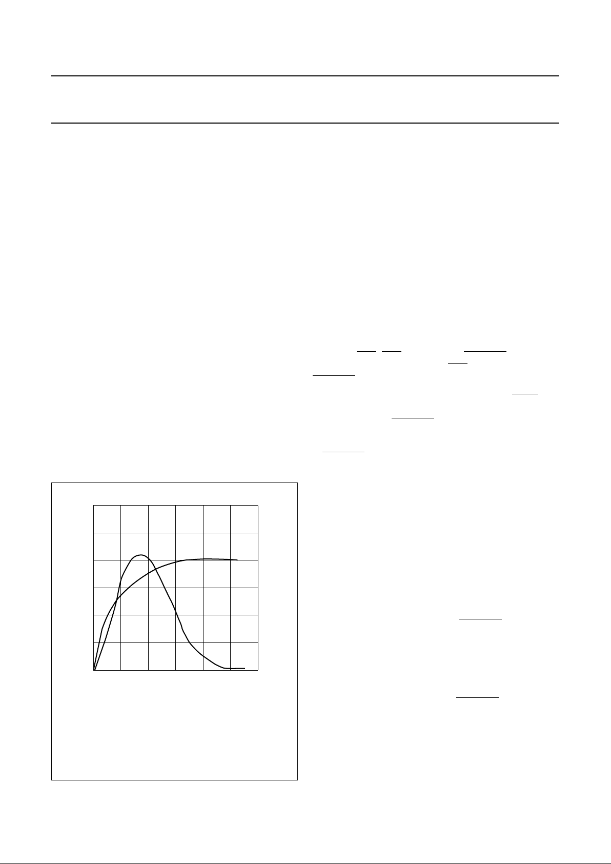
This active pull-up feature ensures fast LOW-to-HIGH
transitions; it is able to deliver more than 1 mA up to an
output voltage of 0.9VCCon a 80 pF load. At the end of the
active pull-up pulse, the output voltage only depends on
the internal pull-up resistor and on the load current (see
Fig.4).
The maximum frequency on these lines is 1 MHz.
Inactive state
Afterpower-onreset,the circuit enters the inactive state. A
minimumnumber of circuits are active while waiting forthe
microcontroller to start a session.
• All card contacts are inactive (approximately 200 Ω to
GND)
• I/OUC, AUX1UC and AUX2UC are high impedance
(10 kΩ pull-up resistor connected to VDD)
• Voltage generators are stopped
• XTAL oscillator is running
• Voltage supervisor is active.
Activation sequence
Afterpower-on and after the internal pulse width delay, the
system controller may check the presence of the card with
the signal OFF (OFF = HIGH while CMDVCC is HIGH
means that the card is present; OFF = LOW while
CMDVCC is HIGH means that no card is present).
If the card is in the reader (which is the case if PRES or
PRES is true), the system controller may start a card
session by pulling CMDVCC LOW.
The following sequence then occurs (see Fig.5):
• CMDVCC is pulled LOW (t0)
• The voltage doubler is started (t1~t0)
• VCC rises from 0 to 5 V with a controlled slope
(t2=t1+1⁄23T) (I/O, AUX1 and AUX2 follow VCC with a
slight delay)
• I/O, AUX1 and AUX2 are enabled (t3=t1+ 4T)
• CLK is applied to the C3 contact (t4)
• RST is enabled (t5=t1+ 7T).
In the timing informations above and below, T is 64 times
the period of the internal oscillator, about 25 µs.
The clock may be applied to the card in the following way:
• Set RSTIN HIGH before setting CMDVCC LOW and
reset it LOW between t3and t5; CLK will start at this
moment. RST will remain LOW until t5, where RST is
enabledto be the copy of RSTIN. After t5,RSTIN has no
further action on CLK. This is to allow a precise count of
CLK pulses before toggling RST.
If this feature is not needed, then CMDVCC may be set
LOWwithRSTINLOW.Inthiscase,CLKwillstart at t3and
after t5,RSTINmaybesetHIGHinordertoget the Answer
To Request (ATR) from the card.
handbook, halfpage
0
(2)
(1)
6
4
2
0
20 40
t (ns)
V
o
(V)
12
8
4
0
I
o
(mA)
60
FCE270
Fig.4 I/O, AUX1, and AUX2 output voltage and
current as a function of time during a
LOW-to-HIGH transition.
(1) Current.
(2) Voltage.
 Loading...