

Philips tda8003ts DATASHEETS

INTEGRATED CIRCUITS
DATA SH EET
TDA8003TS
2
I
C-bus SIM card interface
Product specification
Supersedes data of 2000 Feb 29
File under Integrated Circuits, IC02
2000 Apr 20

Philips Semiconductors Product specification
I2C-bus SIM card interface
FEATURES
• Subscriber Identification Module (SIM) cardinterface in
accordancewithGSM11.11,GSM11.12(GlobalSystem
for Mobile communication) and ISO 7816 requirements
• VCCregulation (3 or 5 V ±8%) with controlled rise and
fall times
• Card take-off protection
• Oneprotectedandbufferedpseudo-bidirectionalI/O line
(I/O referenced to VCC and SIMI/O referenced to V
• Clock generation (up to 10 MHz) with synchronous start
and frequency doubling
• Clock stop LOW, clock stop HIGH or 1.25 MHz (from
internal oscillator) for cards Power-down mode
• Automatic activation and deactivation sequences of an
independent sequencer
• Automatic processing of pin RST with count of the CLK
cycles for start of the Answer To Reset (ATR)
• Warm reset command
• Supply voltage supervisor for Power-on reset, spike
killing and emergency deactivation in case of supply
drop-out
• DC-to-DC converter (doubler, tripler or follower)
allowing operation in a 3 or 5 V environment
(2.5 ≤ VDD≤ 6V)
• EnhancedElectrostatic Discharge (ESD) protections on
card side (6 kV minimum)
• Power-down mode with several active features and
current reduction
• Off mode with 2 µA current
• Control from a microcontroller via a 400 kHz slave
I2C-bus (4 possible addresses: 48H, 4AH, 4CH
and 4EH)
• Four parallel devices possible due to 2 sub-address
wires
• Interface signals supplied by an independent voltage
(1.5 ≤ V
DDI
≤ 6 V).
DDI
TDA8003TS
APPLICATIONS
• GSM mobile phones
)
• SAM interfaces in banking terminals
• Portable card readers, etc.
GENERAL DESCRIPTION
The TDA8003TS is a low cost one chip SIM interface, in
accordance with GSM11.11, GSM11.12 and EMV96
(Europay, Mastercard, Visa) with card current limitation.
Controlled by I2C-bus, it is optimized in terms of board
space, external components count and connection count
(see Chapter “Application information”).
The integrated DC-to-DC converter ensures full
cross-compatibility between 3 or 5 V cards and 3 or 5 V
environments. The very low-power consumption in
Power-down mode and Off mode saves battery power.
ORDERING INFORMATION
TYPE
NUMBER
TDA8003TS/C1 SSOP24 plastic shrink small outline package; 24 leads; body width 5.3 mm SOT340-1
TDA8003TS/C2 SSOP24 plastic shrink small outline package; 24 leads; body width 5.3 mm SOT340-1
2000 Apr 20 2
NAME DESCRIPTION VERSION
PACKAGE
Philips Semiconductors Product specification
I2C-bus SIM card interface
TDA8003TS
QUICK REFERENCE DATA
SYMBOL PARAMETER CONDITIONS MIN. TYP. MAX. UNIT
V
DD
I
DD
supply voltage on pins V
and V
DDP
supply current on pins V
and V
DDP
DDS
DDS
Off mode; VDD=3V −−2µA
Power-down mode; V
DD
=3V;
2.5 − 6V
−−500 µA
VCC=5V; ICC= 100 µA; SIMCLK
connected to PGND or V
DDI
;
CLK is stopped
V
DDI
V
CC
active mode; V
ICC= 6 mA; f
active mode; V
ICC= 10 mA; f
active mode; V
ICC= 6 mA; f
active mode; V
ICC= 10 mA; f
interface signal supply voltage 1.5 − 6V
card supply voltage 5 V card; active mode;
=3V; VCC=3V;
DD
= 3.25 MHz
CLK
= 3 V; VCC=5V;
DD
= 3.25 MHz
CLK
= 5 V; VCC=3V;
DD
= 3.25 MHz
CLK
= 5 V; VCC=5V;
DD
= 3.25 MHz
CLK
−−18 mA
−−50 mA
−−10 mA
−−30 mA
4.6 5 5.4 V
0<ICC< 15 mA; 40 nAs dynamic
load on 200 nF capacitor
3 V card; active mode;
0<I
< 10 mA; 24 nAs dynamic
CC
2.75 3 3.25 V
load on 200 nF capacitor
SR slew rate on V
t
de
t
act
f
i(SIMCLK)
T
amb
deactivation time −−120 µs
activation time −−150 µs
clock input frequency 0 − 20 MHz
operating ambient temperature −40 − +85 °C
(rise and fall) C
CC
5 V card; bit PDOWN = 1; I
3 V card; bit PDOWN = 1; I
= 200 nF 0.05 − 0.25 V/µs
L(max)
< 5 mA 4.6 − 5.4 V
CC
< 5 mA 2.75 − 3.25 V
CC
2000 Apr 20 3

Philips Semiconductors Product specification
I2C-bus SIM card interface
BLOCK DIAGRAM
handbook, full pagewidth
VUP
8
100 nF
3
PGND
100 nF
S3
4
DC-TO-DC
CONVERTER
S4
6
100 nF
S1
2
S2
7
V
DDP
2.2 µF
5
V
DDS
100 nF
14
VOLTAGE
SUPERVISOR
TDA8003TS
21
SIMERR
15
DEL
10 nF
TDA8003TS
SEQUENCER
I/O
12
13
INTERNAL
9
11
16
ANALOG
DRIVERS
AND
PROTECTIONS
OSCILLATOR
10
SGND
I2C-BUS
INTERFACE
AND
REGISTERS
CLOCK
COUNTER
CLOCK
CIRCUITRY
V
CC
200 nF
RST
CLK
PRES
18
23
22
19
20
17
24
MGR434
V
DDI
SAD1
SAD0
SDA
SCL
1
PWROFF
SIMI/O
SIMCLK
Fig.1 Block diagram.
2000 Apr 20 4

Philips Semiconductors Product specification
I2C-bus SIM card interface
TDA8003TS
PINNING
SYMBOL PIN DESCRIPTION
PWROFF 1 control input for entering the Off mode (active LOW)
S1 2 capacitor connection for the DC-to-DC converter (between S1 and S2)
PGND 3 power ground
S3 4 capacitor connection for the DC-to-DC converter (between S3 and S4)
V
DDP
5 power supply voltage
S4 6 capacitor connection for the DC-to-DC converter (between S3 and S4)
S2 7 capacitor connection for the DC-to-DC converter (between S1 and S2)
VUP 8 DC-to-DC converter output (must be decoupled with 100 nF to ground)
I/O 9 input/output to and from the card reader (C7I); see Fig.7
SGND 10 signal ground
CLK 11 clock output to the card reader (C3I)
V
CC
12 supply voltage to the card reader (C1I)
RST 13 reset output to the card reader (C2I)
V
DDS
14 signal supply voltage
DEL 15 external capacitor connection for the delay on voltage supervisor
PRES 16 card presence indication input (active LOW); note 1
SIMI/O 17 input/output to and from the microcontroller (internal 20 kΩ pull-up resistor connected to V
V
DDI
SDA 19 I
SCL 20 I
SIMERR 21 interrupt output (active LOW; internal 100 kΩ pull-up resistor connected to V
SAD0 22 I
SAD1 23 I
18 supply voltage for the interface signals with the system
2
C-bus serial data input/output
2
C-bus serial clock input
2
C-bus slave address selection input
2
C-bus slave address selection input
DDI
)
SIMCLK 24 external clock input
DDI
)
Note
1. Card presence input with negative current source. To be used with the card reader switch connected to V
or V
. The switch is normally closed when the card is not present. If the switch connection is open-circuit or pin 16
DDP
is not connected, then the interface will always detect a present card (see Fig.7).
2000 Apr 20 5
DDS

Philips Semiconductors Product specification
I2C-bus SIM card interface
handbook, halfpage
PWROFF
S1
PGND
S3
V
DDP
S4
S2
VUP
I/O
SGND
CLK
V
CC
1
2
3
4
5
6
TDA8003TS
7
8
9
10
11
12
MGR435
24
23
22
21
20
19
18
17
16
15
14
13
SIMCLK
SAD1
SAD0
SIMERR
SCL
SDA
V
DDI
SIMI/O
PRES
DEL
V
DDS
RST
TDA8003TS
Fig.2 Pin configuration.
FUNCTIONAL DESCRIPTION
Figure 1 shows the block diagram of the TDA8003TS.
The functional blocks are described in the following
sections. It is assumed that the reader of this specification
is aware of GSM11.11 and ISO 7816 terminology.
2
C-bus control
I
The I2C-bus interface is used:
• To configure the clock to the card in active mode
(1⁄2f
SIMCLK
and1⁄4f
SIMCLK
)
• To configure the clock to the card in power reduction
mode (stop LOW, stop HIGH or ±1.25 MHz derived
from the internal oscillator)
• To select operation with a 3 or 5 V card
• To start or stop sessions (cold reset)
• To initiate a warm reset
• To enter or leave the Power-down mode
• To request the status (card present or not, hardware
problem occurred, unresponsive card after activation,
supplydrop-outdetected by the voltage supervisor, card
powered or not)
• To configure SIMI/O and I/O in high-impedance (for use
of several TDA8003TS in parallel).
The structure of the I
2
C-bus data frames is as follows:
• Commands to the TDA8003TS:
– START/ADDRESS/WRITE
– COMMAND BYTE
– STOP.
The fixed address is 01001XY. X and Y are defined by
the logic levels on pins SAD1 and SAD0 as shown in
Table 1 (connect to ground for logic 0; connect to V
for logic 1). The command bits are described in Table 2.
The commands are executed on the rising edge of the
9th SCL pulse.
• Status from the TDA8003TS (see Table 4). The fixed
address is 01001XY. X and Y are defined by the logic
levels on pins SAD1 and SAD0 as shown in Table 1.
Table 1 Address selections
ADDRESS SAD1 SAD0
48H 0 0
4AH 0 1
4CH 1 0
4EH 1 1
DDI
2000 Apr 20 6
Philips Semiconductors Product specification
I2C-bus SIM card interface
TDA8003TS
Table 2 Description of the command bits; (all bits are cleared at reset)
SYMBOL BIT DESCRIPTION
START/STOP 0 Logic1 initiates an activation sequence and a cold reset procedure. Logic 0 initiates a
deactivation sequence.
WARM 1 Logic 1 initiates a warm reset procedure. TDA8003TS/C1:warm reset performed only
when the 2 times 45000 CLK pulses have expired without answer from the card.
TDA8003TS/C2:warm reset performed whateverthe card has answered or not at the
cold reset procedure but the count is 2 times 44745 CLK pulses.
3 V/5 VN 2 Logic 1 sets the card supply voltage V
to 3 V. Logic 0 sets VCC to 5 V.
CC
PDOWN 3 Logic 1 applies on CLK the frequency defined by bits CLKPD1 and CLKPD2, and
enters a reduced consumption mode. Logic 0 sets the circuit back to normal mode.
CLKPD1 4 Bits 4 and 5 determine the clock to the card at power-down as shown in Table 3.
CLKPD2 5
DT/DFN 6 Logic 1 sets f
CLK
to1⁄2f
(in active mode). Logic 0 sets f
SIMCLK
CLK
to1⁄4f
SIMCLK
.
I/OEN 7 Logic 1 will transfer I/O to SIMI/O. Logic 0 sets I/O and SIMI/O to high-impedance.
Table 3 Clock to the card at power-down
BIT 4 BIT 5 FUNCTION
0 0 clock stop LOW
0 1 clock stop HIGH
1 0 clock is
1
⁄2f
osc
1 1 no change
Table 4 Description of the status bits; note 1
SYMBOL BIT DESCRIPTION
PRES 0 Logic 1 when the card is present. Logic 0 when the card is not present.
PRESL 1 Logic 1 when the card has been extracted or inserted. Logic 0 when the status is
read-out.
− 2 Bit 2 is not used and is fixed to logic 0.
SUPL 3 Logic 1 when the voltage supervisor has signalled a fault. Logic 0 when the status is
read-out.
PROT 4 Logic 1 when an overload has occurred during a session. Logic 0 when the status is
read-out.
MUTE 5 TDA8003TS/C1: Logic 1 when a card has not answered after 2 times 45000 CLK
pulses. Logic 0 when the status is read-out.
TDA8003TS/C2: Same as for C1, but the count is 2 times 44745 CLK pulses.
EARLY 6 Logic 1 when a card has answered between 200 and 352 CLK cycles. Logic 0 when
the status is read-out.
ACTIVE 7 Logic 1 when the card is power-on. Logic 0 when the card is power-off.
Note
1. In case of card extraction, supply drop-out or overload detection within a session, the card will be automatically
deactivated, SIMERR pulled LOW, bit START = 0 and the corresponding status bit = 1. The status bit will be logic 0
and SIMERR will be released when the microcontroller reads out the status register, on the 7th SCL pulse. After a
supply drop-out, SIMERR will be released at the end of the alarm pulse and bit SUPL = 1.
2000 Apr 20 7
Philips Semiconductors Product specification
I2C-bus SIM card interface
Power supply
The circuit operates within a supply voltage range of
2.5 to 6 V. The supply pins are V
V
and PGND only supply the DC-to-DC converter for
DDP
the analog drivers to the card and must be decoupled
externallybecauseofthe large current spikes that the card
and the DC-to-DC converter can create. An integrated
spike killer ensures the card contacts to remain inactive
during power-up or power-down. An internal voltage
reference is generated for the DC-to-DC converter, the
voltage supervisor and the VCC generator.
All interface signals with the microcontroller (PWROFF,
SIMCLK, SAD1, SAD0, SIMERR, SCL, SDA and SIMI/O)
are referenced to a separate supply pin V
be different from VDD (1.5 ≤ V
DDI
The pull-up resistors on bus lines SDA and SCL may be
referenced to a voltage higher than V
use of peripherals which do not operate at V
and SGND. Pins
DDS
DDI
≤ 6 V).
. This allows the
DDI
, which may
.
DDI
TDA8003TS
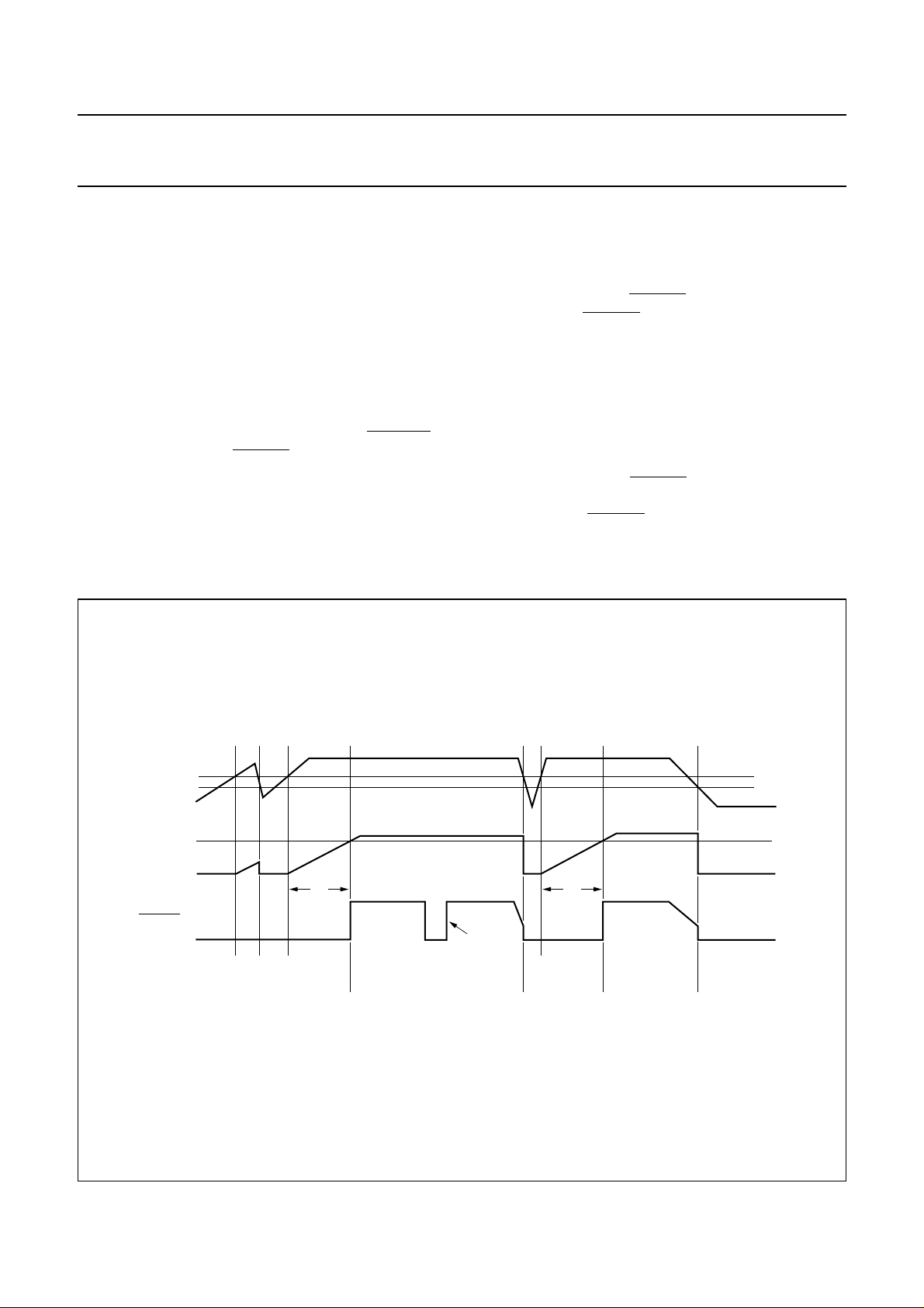
The voltage supervisor (see Fig.3) senses V
generates an alarm pulse, whose length tW is defined by
an external capacitor connected to pin DEL, when VDD is
too low to ensure proper operation (1 ms per 1 nF typical).
During this alarm pulse, SIMERR is LOW and the I2C-bus
is unresponsive. SIMERR goes back to HIGH, and the
I2C-bus becomes operational at the end of this alarm
pulse. Bit SUPL is set as long as the status has not been
read.
It is also used to either block any spurious signals on card
contacts during microcontroller reset, or to force an
automatic deactivation of the contacts in the event of
supply drop-out.
Outside a card session, SIMERR is LOW as long as the
voltage supervisor is active. If a supply drop-out occurs
during a session, SIMERR falls to LOW, bit START is
cleared and an automatic deactivation is initiated.
DDS
. It
handbook, full pagewidth
V
DDS
DEL
SIMERR
2
I
C-bus unresponsive
t
W
status read
after event
2
I
C-bus OK
t
W
2
C-bus
I
unresponsive
I2C-bus OK
I2C-bus
unresponsive
MGR436
Fig.3 Voltage supervisor.
2000 Apr 20 8
 Loading...