

Philips TDA8002CG-C1, TDA8002CT-C-C1, TDA8002CT-B-C1, TDA8002CT-A-C1 Datasheet

INTEGRATED CIRCUITS
DATA SH EET
TDA8002C
IC card interface
Product specification
Supersedes data of 1999 Feb 24
File under Integrated Circuits, IC02
1999 Oct 12
Philips Semiconductors Product specification
IC card interface TDA8002C
FEATURES
• Single supply voltageinterface(3.3 or 5 V environment)
• Low-power sleep mode
• Three specific protected half-duplex bidirectional
buffered I/O lines
• VCC regulation 5 V ±5% or 3 V ±5%, ICC<55mAfor
VDD= 3.0 to 6.5 V, with controlled rise and fall times
• Thermal and short-circuit protections with current
limitations
• Automatic ISO 7816 activation and deactivation
sequences
• Enhanced ESD protections on card side (>6 kV)
• Clock generation for the card up to 12 MHz with
synchronous frequency changes
• Clock generation up to 20 MHz (external clock)
• Synchronous and asynchronous cards (memory and
smart cards)
• ISO 7816, GSM11.11 compatibility and EMV
(Europay, MasterCard and Visa) compliant
• Step-up converter for VCC generation
• Supplysupervisor for spikes eliminationand emergency
deactivation
• Chip select input for easy use of several TDA8002Cs in
parallel.
APPLICATIONS
IC card readers for:
• GSM applications
• Banking
• Electronic payment
• Identification
• Pay TV
• Road tolling.
GENERAL DESCRIPTION
The TDA8002C is a complete low-power analog interface
forasynchronous and synchronous cards.Itcan be placed
between the card and the microcontroller. It performs all
supply, protection and control functions. It is directly
compatible with ISO 7816, GSM11.11 and EMV
specifications.
ORDERING INFORMATION
TYPE NUMBER
TDA8002CT/A/C1 TDA8002CT/A SO28 plastic small outline package; 28 leads; body width
TDA8002CT/B/C1 TDA8002CT/B
TDA8002CT/C/C1 TDA8002CT/C
TDA8002CG/C1 TDA8002C LQFP32 plastic low profile quad flat package; 32 leads;
MARKING NAME DESCRIPTION VERSION
7.5 mm
body 5 × 5 × 1.4 mm
PACKAGE
SOT136-1
SOT401-1
1999 Oct 12 2

Philips Semiconductors Product specification
IC card interface TDA8002C
QUICK REFERENCE DATA
SYMBOL PARAMETER CONDITIONS MIN. TYP. MAX. UNIT
Supplies
V
DD
I
DD(lp)
I
DD(idle)
I
DD(active)
Card supply
V
CC(O)
General
f
CLK
t
de
P
tot
T
amb
supply voltage 3.0 − 6.5 V
supply current low-power −−150 µA
supply current Idle mode; f
CLKOUT
supply current active mode; V
f
CLKOUT
=10MHz
= LOW; ICC= 100 µA −−8mA
f
CLK
f
= 5 MHz; ICC=10mA −−50 mA
CLK
f
= 5 MHz; ICC=55mA −−140 mA
CLK
active mode; V
f
CLKOUT
=10MHz
f
= LOW; ICC= 100 µA −−8mA
CLK
f
= 5 MHz; ICC=10mA −−50 mA
CLK
f
= 5 MHz; ICC=55mA −−140 mA
CLK
= 10 MHz −−5mA
=5V;
CC(O)
=3V;
CC(O)
output voltage active mode for VCC=5V
I
< 55 mA; DC load 4.6 − 5.4 V
CC
= 40 nAs; AC load 4.6 − 5.4 V
I
CC
active mode for V
I
< 55 mA; DC load 2.76 − 3.24 V
CC
= 40 nAs; AC load 2.76 − 3.24 V
I
CC
CC
=3V
card clock frequency 0 − 12 MHz
deactivation sequence duration 60 80 100 µs
continuous total power dissipation
TDA8002CT/x T
TDA8002CG T
= −25 to +85 °C −−0.56 W
amb
= −25 to +85 °C −−0.46 W
amb
ambient temperature −25 − +85 °C
1999 Oct 12 3

Philips Semiconductors Product specification
IC card interface TDA8002C
BLOCK DIAGRAM
handbook, full pagewidth
ALARM
CS
OFF
RSTIN
CMDVCC
MODE
CV/TV
CLKDIV1
CLKDIV2
CLKSEL
STROBE
V
DDD
100 nF
28
SUPPLY
INTERNAL
4
3
26
25
24
27
19
6
7
5
8
REFERENCE
VOLTAGE SENSE
ALARM
LATCH
CLOCK
CIRCUITRY
V
V
ref
SEQUENCER
DDA
S1 S2
14 12
2.5 MHz
EN2
PV
CC
EN5
EN4
470 nF
GENERATOR
100 nF
13
STEP-UP CONVERTER
INTERNAL OSCILLATOR
EN1 CLKUP
V
CC
RST
BUFFER
CLOCK
BUFFER
AGND
11
VUP
15
470 nF
V
100
nF
CC
23
100
nF
22
21
18
RST
CLK
PRES
CLKOUT
XTAL1
XTAL2
AUX1UC
9
CLK
30
31
1
OSCILLATOR
EN3
TDA8002CG
AUX2UC
I/OUC
2
32
10
DGND1
29
DGND2
Fig.1 Block diagram.
1999 Oct 12 4
THERMAL
PROTECTION
TRANSCEIVER
TRANSCEIVER
TRANSCEIVER
I/O
I/O
I/O
20
17
16
FCE246
AUX1
AUX2
I/O

Philips Semiconductors Product specification
IC card interface TDA8002C
PINNING
PIN
SYMBOL
TYPE
CT/A
TYPE
CT/B
TYPE
CT/C
TYPE
CG
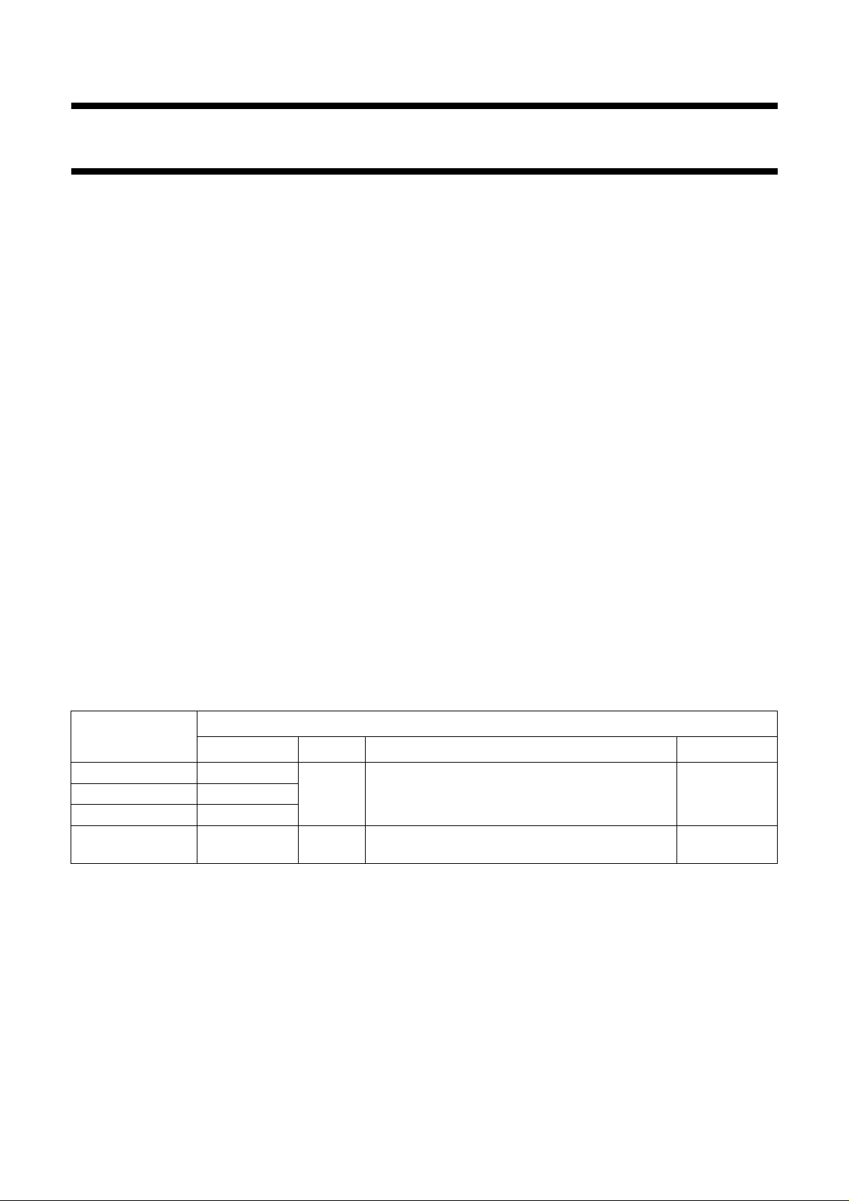
XTAL1 1 1 1 30 I crystal connection or input for external clock
XTAL2 2 2 2 31 O crystal connection
I/OUC 3 3 3 32 I/O data I/O line to and from microcontroller
AUX1UC 4441I/Oauxiliary line 1 to and from microcontroller for synchronous
AUX2UC 5 −−2 I/O auxiliary line 2 to and from microcontroller for synchronous
CS − 5 5 3 I chip select control input for enabling pins I/OUC, AUX1UC,
ALARM 6664Oopen drain PMOS reset output for microcontroller (active
CLKSEL 7775Icontrol input signal for CLK (LOW = XTAL oscillator;
CLKDIV1 8886Icontrol input with CLKDIV2 for choosing CLK frequency
CLKDIV2 9997Icontrol input with CLKDIV1 for choosing CLK frequency
STROBE 10 10 10 8 I external clock input for synchronous applications
CLKOUT 11 11 11 9 O clock output (see Table 1)
DGND1 12 12 12 10 supply digital ground 1
AGND 13 13 13 11 supply analog ground
S2 14 14 14 12 I/O capacitance connection for voltage doubler
V
DDA
15 15 15 13 supply analog supply voltage
S1 16 16 16 14 I/O capacitance connection for voltage doubler
VUP 17 17 17 15 I/O output of voltage doubler
I/O 18 18 18 16 I/O data I/O line to and from card
AUX2 19 −−17 I/O auxiliary I/O line to and from card
PRES 20 19 19 18 I card input presence contact (active LOW)
PRES − 20 −−I active HIGH card input presence contact
CV/
TV −−20 19 I card voltage selection input line (high = 5 V, low = 3 V); note 1
AUX1 21 21 21 20 I/O auxiliary I/O line to and from card
CLK 22 22 22 21 O clock to card output (C3I) (see Table 1)
RST 23 23 23 22 O card reset output (C2I)
V
CC
24 24 24 23 O supply for card (C1I)
CMDVCC 25 25 25 24 I start activation sequence input from microcontroller (active
RSTIN 26 26 26 25 I card reset input from microcontroller
OFF 27 27 27 26 O open-drain NMOS interrupt output to microcontroller (active
I/O DESCRIPTION
applications
applications
AUX2UC, CLKSEL, CLKDIV1, CLKDIV2, STROBE, CV/
CMDVCC, RSTIN, OFF and MODE; note 1
HIGH)
HIGH = STROBE input)
LOW)
LOW)
TV,
1999 Oct 12 5

Philips Semiconductors Product specification
IC card interface TDA8002C
PIN
SYMBOL
TYPE
CT/A
TYPE
CT/B
TYPE
CT/C
TYPE
CG
MODE 28 28 28 27 I operating mode selection input (HIGH = normal; LOW = sleep)
V
DDD
−−−28 supply digital supply voltage
DGND2 −−−29 supply digital ground 2
Note
1. A pull-up resistor of 100 kΩ connected to VDD is integrated.
I/O DESCRIPTION
handbook, halfpage
AUX1UC
AUX2UC
CLKSEL
CLKDIV1
CLKDIV2
STROBE
CLKOUT
Fig.2 Pin configuration (TDA8002CT/A).
XTAL1
XTAL2
I/OUC
ALARM
DGND1
AGND
S2
1
2
3
4
5
6
7
TDA8002CT/A
8
9
10
11
12
13
FCE247
28
27
26
25
24
23
22
21
20
19
18
17
16
1514
MODE
OFF
RSTIN
CMDVCC
V
CC
RST
CLK
AUX1
PRES
AUX2
I/O
VUP
S1
V
DDA
handbook, halfpage
AUX1UC
CLKSEL
CLKDIV1
CLKDIV2
STROBE
CLKOUT
Fig.3 Pin configuration (TDA8002CT/B).
XTAL1
XTAL2
I/OUC
CS
ALARM
DGND1
AGND
S2
1
2
3
4
5
6
7
TDA8002CT/B
8
9
10
11
12
13
FCE248
28
27
26
25
24
23
22
21
20
19
18
17
16
1514
MODE
OFF
RSTIN
CMDVCC
V
CC
RST
CLK
AUX1
PRES
PRES
I/O
VUP
S1
V
DDA
1999 Oct 12 6
Philips Semiconductors Product specification
IC card interface TDA8002C
handbook, halfpage
AUX1UC
CLKSEL
CLKDIV1
CLKDIV2
STROBE
CLKOUT
Fig.4 Pin configuration (TDA8002CT/C).
Fig.4 Pin configuration (TDA8002CT/C).
XTAL1
XTAL2
I/OUC
CS
ALARM
DGND1
AGND
S2
1
2
3
4
5
6
7
TDA8002CT/C
8
9
10
11
12
13
FCE249
28
27
26
25
24
23
22
21
20
19
18
17
16
1514
MODE
OFF
RSTIN
CMDVCC
V
CC
RST
CLK
AUX1
CV/TV
PRES
I/O
VUP
S1
V
DDA
handbook, full pagewidth
AUX1UC
AUX2UC
CS
ALARM
CLKSEL
CLKDIV1
CLKDIV2
STROBE
XTAL2
I/OUC
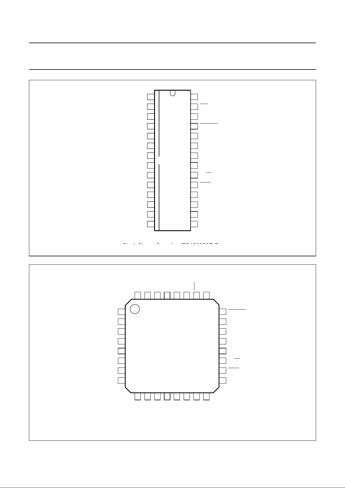
32
1
2
3
4
XTAL1
31
30
V
DGND2
29
DDD
28
MODE
27
OFF
26
TDA8002CG
5
6
7
8
9
CLKOUT
10
DGND1
11
AGND
12
S2
13
DDA
V
14
S1
15
VUP
Fig.5 Pin configuration (TDA8002CG).
RSTIN
25
16
I/O
24
23
22
21
20
19
18
17
FCE250
CMDVCC
V
CC
RST
CLK
AUX1
CV/TV
PRES
AUX2
1999 Oct 12 7

Philips Semiconductors Product specification
IC card interface TDA8002C
FUNCTIONAL DESCRIPTION
Power supply
The supply pins for the chip are V
DGND1 and DGND2. V
DDA
and V
, V
DDA
DDD
, AGND,
DDD
(i.e. VDD) should be
in the range of 3.0 to 6.5 V. All card contacts remain
inactive during power-up or power-down.
On power-up, the logic is reset by an internal signal.
The sequencer is not activated until VDD reaches
V
th2+Vhys2
(see Fig.6). When VDD falls below V
th2
, an
automatic deactivation sequence of the contacts is
performed.
Chip selection
The chip select pin (CS) allows the use of several
TDA8002Cs in parallel.
When CS is HIGH, the pins RSTN, CMDVCC, MODE,
CV/TV, CLKDIV1, CLKDIV2, CLKSEL and STROBE
control the chip, pins I/OUC, AUX1UC and AUX2UC are
the copy of I/O, AUX1 and AUX2 when enabled (with
integrated 20 kΩ pull-up resistors connected to VDD) and
OFF is enabled.
When CS goes LOW, the levels on pins RSTIN,
CMDVCC, MODE, CV/TV, CLKDIV1, CLKDIV2 and
STROBE are internally latched, I/OUC, AUX1UC and
AUX2UC go to high-impedance with respect to I/O, AUX1
and AUX2 (with integrated 100 kΩ pull-up resistors
connected to VDD) and OFF is high-impedance.
Clock circuitry
The TDA8002C supports both synchronous and
asynchronouscards. There arethree methods to clockthe
circuitry:
• Apply a clock signal to pin STROBE
• Use of an internal RC oscillator
• Use of a quartz oscillator which should be connected
between pins XTAL1 and XTAL2 or an external clock
applied on XTAL1.
When CLKSEL is HIGH, the clock should be applied to the
STROBE pin. When CLKSEL is LOW, the internal
oscillators is used.
When an internal clock is used, the clock output is
availableon pin CLKOUT.The RC oscillator is selectedby
making CLKDIV1 HIGH and CLKDIV2 LOW. The clock
output to the card is available on pin CLK. The frequency
of the card clock can be the input frequency divided by
2 or 4, STOP low or 1.25 MHz, depending onthe states of
CLKDIV1 or CLKDIV2 (see Table 1).
When STROBE is used for entering the clock to a
synchronous card, STROBE should remain stable during
activation sequence otherwise the first pulse may be
omitted.
Do not change CLKSEL during activation. When in
low-power (sleep) mode, the internal oscillator frequency
which is available on pin CLKOUT is lowered to
approximately 16 kHz for power economy purposes.
Supply voltage supervisor (VDD)
This block surveys the V
supply. A defined retriggerable
DD
pulse of 10 ms minimum (tW) is delivered on the ALARM
output during power-up or power-down of VDD(see Fig.6).
This signal is also used for eliminating the spikes on card
contacts during power-up or power-down.
When VDD reaches V
th2+Vhys2
, an internal delay (tW) is
started. The ALARM output is active until this delay has
expired. When VDD falls below V
, ALARM is activated
th2
and a deactivation sequence of the contacts is performed.
1999 Oct 12 8

Philips Semiconductors Product specification
IC card interface TDA8002C
handbook, full pagewidth
V
+ V
th2
V
DD
hys2
V
th2
handbook, full pagewidth
OFF, I/OUC
AUX1UC, AUX2UC
ALARM
t
W
t
W
FCE272
Fig.6 ALARM as a function of VDD (tWpulse width minimum of 10 ms).
CS
t
SL
CS
INPUTS
t
t
IS
SI
Fig.7 Chip select.
1999 Oct 12 9
t
DZ
t
t
ID
DI
FCE245
 Loading...