

Philips TDA8025, TDA8023, TDA8002BT-5-C2, TDA8002BT-5, TDA8002BT-3 Datasheet
...
INTEGRATED CIRCUITS
DATA SH EET
TDA8002
IC card interface
Product specification
Supersedes data of 1997 Mar 13
File under Integrated Circuits, IC02
1997 Nov 04

Philips Semiconductors Product specification
IC card interface TDA8002
FEATURES
• Single supply voltage interface (3.3 or 5 V environment)
• Low-power sleep mode
• Three specific protected half-duplex bidirectional
buffered I/O lines
• VCC regulation (5 V ±5%, ICC<65 mA at VDD= 5 V, with
controlled rise and fall times
• Thermal and short-circuit protections with current
limitations
• Automatic ISO 7816 activation and deactivation
sequences
• Enhanced ESD protections on card side (>6 kV)
• Clock generation for the card up to 12 MHz with
synchronous frequency changes
• Clock generation up to 20 MHz (auxiliary clock)
• Synchronous and asynchronous cards (memory and
smart cards)
• ISO 7816, GSM11.11 compatibility and EMV (Europay,
Mastercard, Visa) compliant
• Step-up converter for V
generation
CC
• Supply supervisor for spikes elimination and emergency
deactivation.
APPLICA TIONS
• IC card readers for:
– GSM applications
– banking
– electronic payment
– identification
– Pay TV
– road tolling.
GENERAL DESCRIPTION
The TDA8002 is a complete low-power, analog interface
for asynchronous and synchronous cards. It can be placed
between the card and the microcontroller. It performs all
supply, protection and control functions. It is directly
compatible with ISO 7816, GSM11.11 and EMV
specifications.
QUICK REFERENCE DATA
SYMBOL PARAMETER CONDITIONS MIN. TYP. MAX. UNIT
Supply
V
I
DDA
DD
analog supply voltage 3.0 5 6.5 V
supply current sleep mode −−150 µA
idle mode; f
f
CLKOUT
= 10 MHz; VDD=5V
active mode; f
f
CLKOUT
= 10 MHz; VDD=5V
active mode; f
f
CLKOUT
= 10 MHz; VDD=3V
= 2.5 MHz;
CLK
CLK
CLK
= 2.5 MHz;
= 2.5 MHz;
−−6mA
−−9mA
−−12 mA
Card supply
V
CC(O)
I
CC(O)
output voltage DC load <65 mA 4.75 − 5.25 V
output current VCC short-circuited to GND −−100 mA
General
f
CLK
T
P
T
de
tot
amb
card clock frequency 0 − 12 MHz
deactivation cycle time 60 80 100 µs
continuous total power dissipation
TDA8002AT; TDA8002BT T
TDA8002G T
= −25 to +85 °C −−0.56 W
amb
= −25 to +85 °C −−0.46 W
amb
operating ambient temperature −25 − +85 °C
1997 Nov 04 2
Philips Semiconductors Product specification
IC card interface TDA8002
ORDERING INFORMATION
TYPE NUMBER
(1)
PACKAGE
MARKING NAME DESCRIPTION VERSION
TDA8002AT/3/C2
TDA8002AT/5/C2
TDA8002BT/3/C2
TDA8002BT/5/C2
TDA8002G/3/C2
TDA8002G/5/C2
TDA8002AT/3 SO28 plastic small outline package; 28 leads;
(3)
TDA8002AT/5
(2)
TDA8002BT/3
(3)
TDA8002BT/5
(2)
80023 LQFP32 plastic low profile quad flat package; 32 leads;
(3)
80025
body width 7.5 mm
body 5 × 5 × 1.4 mm
SOT136-1
SOT401-1
(2)
Notes
1. The /3 or /5 suffix indicates the voltage supervisor option.
2. The /3 version can be used with a 3 or 5 V power supply environment (see Chapter “Functional description”).
3. The /5 version can be used with a 5 V power supply environment.
1997 Nov 04 3
Philips Semiconductors Product specification
IC card interface TDA8002
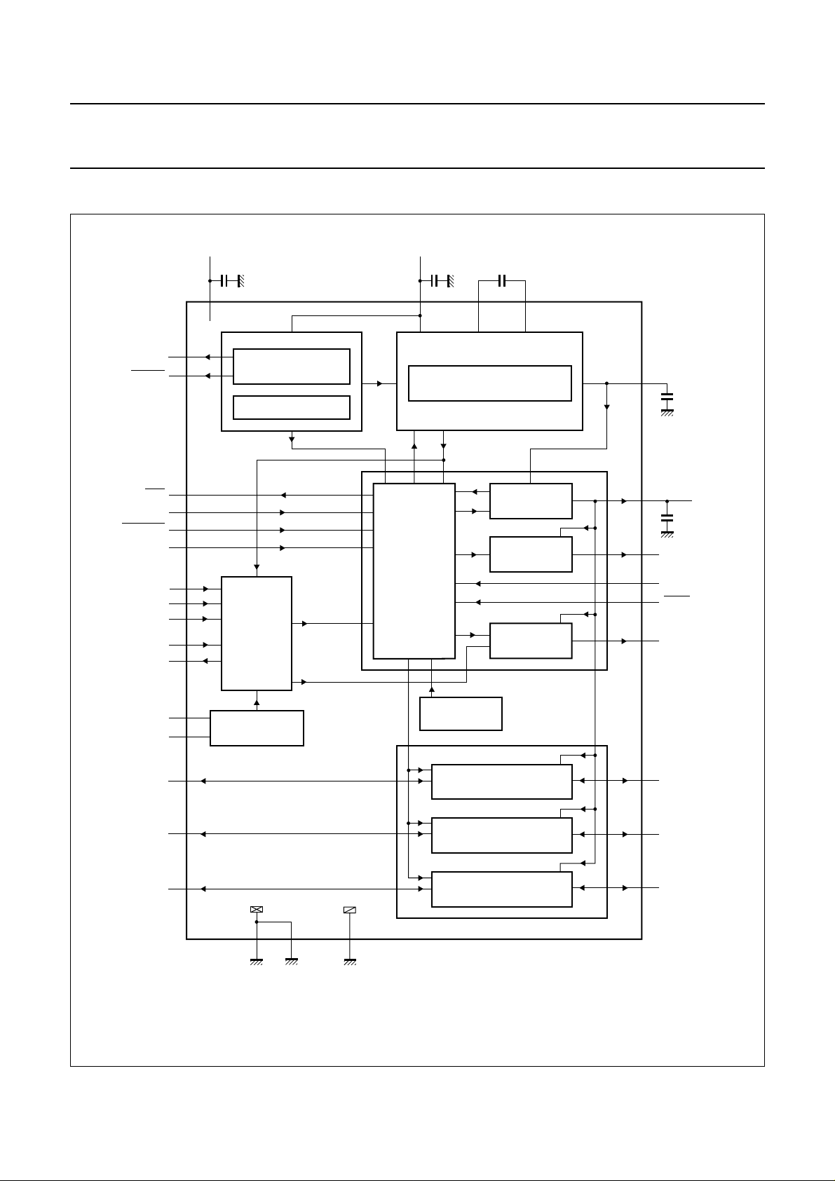
BLOCK DIAGRAM
handbook, full pagewidth
ALARM
ALARM
OFF
RSTIN
CMDVCC
MODE
CLKDIV1
CLKDIV2
CLKSEL
STROBE
CLKOUT
4
3
26
25
24
27
6
7
5
8
9
V
DDD
100 nF
28
CLOCK
CIRCUITRY
SUPPLY
INTERNAL
REFERENCE
VOLTAGE SENSE
HORSEQ
CLK
V
REF
ALARM
V
DDA
100 nF
13
INTERNAL OSCILLATOR
EN1 CLKUP
SEQUENCER
100 nF
S1 S2
14 12
STEP-UP CONVERTER
f
INT
EN2
PV
EN5
EN4
CC
V
CC
GENERATOR
RST
BUFFER
CLOCK
BUFFER
VUP
15
100 nF
23
22
19
18
21
100
RST
PRES
PRES
CLK
nF
V
CC
XTAL1
XTAL2
AUX1UC
30
31
1
OSCILLATOR
EN3
TDA8002G
AUX2UC
I/OUC
All capacitors are mandatory.
2
32
29 11
10
DGND1
DGND2
AGND
Fig.1 Block diagram (TDA8002G).
1997 Nov 04 4
THERMAL
PROTECTION
TRANSCEIVER
TRANSCEIVER
TRANSCEIVER
I/O
I/O
I/O
20
17
16
MGE730
AUX1
AUX2
I/O

Philips Semiconductors Product specification
IC card interface TDA8002
PINNING
SYMBOL
I/O DESCRIPTION
TYPE A TYPE B TYPE G
XTAL1 1 1 30 I/O crystal connection or input for external clock
XTAL2 2 2 31 I/O crystal connection
I/OUC 3 3 32 I/O data I/O line to and from microcontroller
AUX1UC 4 4 1 I/O auxiliary line to and from microcontroller for synchronous
applications
AUX2UC 5 − 2 I/O auxiliary line to and from microcontroller for synchronous
applications
ALARM − 5 3 O open drain NMOS reset output for microcontroller (active LOW)
ALARM 6 6 4 O open drain PMOS reset output for microcontroller (active
HIGH)
CLKSEL 7 7 5 I control input signal for CLK (LOW = XTAL oscillator;
HIGH = STROBE input)
CLKDIV1 8 8 6 I control input with CLKDIV2 for choosing CLK frequency
CLKDIV2 9 9 7 I control input with CLKDIV1 for choosing CLK frequency
STROBE 10 10 8 I external clock input for synchronous applications
CLKOUT 11 11 9 O clock output (see Table 1)
DGND1 12 12 10 supply digital ground 1
AGND 13 13 11 supply analog ground
S2 14 14 12 I/O capacitance connection for voltage doubler
PIN
V
DDA
15 15 13 supply analog supply voltage
S1 16 16 14 I/O capacitance connection for voltage doubler
VUP 17 17 15 I/O output of voltage doubler (connect to 100 nF)
I/O 18 18 16 I/O data I/O line to and from card
AUX2 19 − 17 I/O auxiliary I/O line to and from card
PRES 20 19 18 I active LOW card input presence contact
PRES − 20 19 I active HIGH card input presence contact
AUX1 21 21 20 I/O auxiliary I/O line to and from card
CLK 22 22 21 O clock to card output (C3) (see Table 1)
RST 23 23 22 O card reset output (C2)
V
CC
24 24 23 O supply for card (C1) (decouple with 100 nF)
CMDVCC 25 25 24 I active LOW start activation sequence input from
microcontroller
RSTIN 26 26 25 I card reset input from microcontroller
OFF 27 27 26 O open drain NMOS interrupt output to microcontroller (active
LOW)
MODE 28 28 27 I operating mode selection input (HIGH = normal; LOW = sleep)
V
DDD
−−28 supply digital supply voltage
DGND2 −−29 supply digital ground 2
1997 Nov 04 5

Philips Semiconductors Product specification
IC card interface TDA8002
handbook, halfpage
Fig.2 Pin configuration (TDA8002A).
XTAL1
XTAL2
I/OUC
AUX1UC
AUX2UC
ALARM
CLKSEL
CLKDIV1
CLKDIV2
STROBE
CLKOUT
DGND1
AGND
S2
1
2
3
4
5
6
7
TDA8002A
8
9
10
11
12
13
MGE731
28
27
26
25
24
23
22
21
20
19
18
17
16
1514
MODE
OFF
RSTIN
CMDVCC
V
CC
RST
CLK
AUX1
PRES
AUX2
I/O
VUP
S1
V
DDA
handbook, halfpage
CLKDIV1
CLKDIV2
STROBE
Fig.3 Pin configuration (TDA8002B).
XTAL1
XTAL2
I/OUC
AUX1UC
ALARM
ALARM
CLKSEL
CLKOUT
DGND1
AGND
S2
1
2
3
4
5
6
7
TDA8002B
8
9
10
11
12
13
MGE732
28
27
26
25
24
23
22
21
20
19
18
17
16
1514
MODE
OFF
RSTIN
CMDVCC
V
CC
RST
CLK
AUX1
PRES
PRES
I/O
VUP
S1
V
DDA
handbook, full pagewidth
AUX1UC
AUX2UC
ALARM
ALARM
CLKSEL
CLKDIV1
CLKDIV2
STROBE
XTAL2
I/OUC
32
1
2
3
4
XTAL1
31
30
DGND2
29
DDD
V
28
MODE
27
OFF
26
TDA8002G
5
6
7
8
9
CLKOUT
10
DGND1
11
AGND
S2
12
13
14
15
S1
DDA
V
VUP
Fig.4 Pin configuration (TDA8002G).
RSTIN
25
16
I/O
CMDVCC
24
V
23
RST
22
21
CLK
20
AUX1
19
PRES
18
PRES
17
AUX2
MGE733
CC
1997 Nov 04 6
Philips Semiconductors Product specification
IC card interface TDA8002
FUNCTIONAL DESCRIPTION
Power supply
The supply pins for the chip are V
DGND1 and DGND2. V
DDA
and V
, V
DDA
DDD
, AGND,
DDD
(i.e. VDD) should be
in the range of 3.0 to 6.5 V. All card contacts remain
inactive during power-up or power-down.
On power-up, the logic is reset by an internal signal.
The sequencer is not activated until VDD reaches
V
th2+Vhys2
(see Fig.5). When VDD falls below V
th2
, an
automatic deactivation sequence of the contacts is
performed.
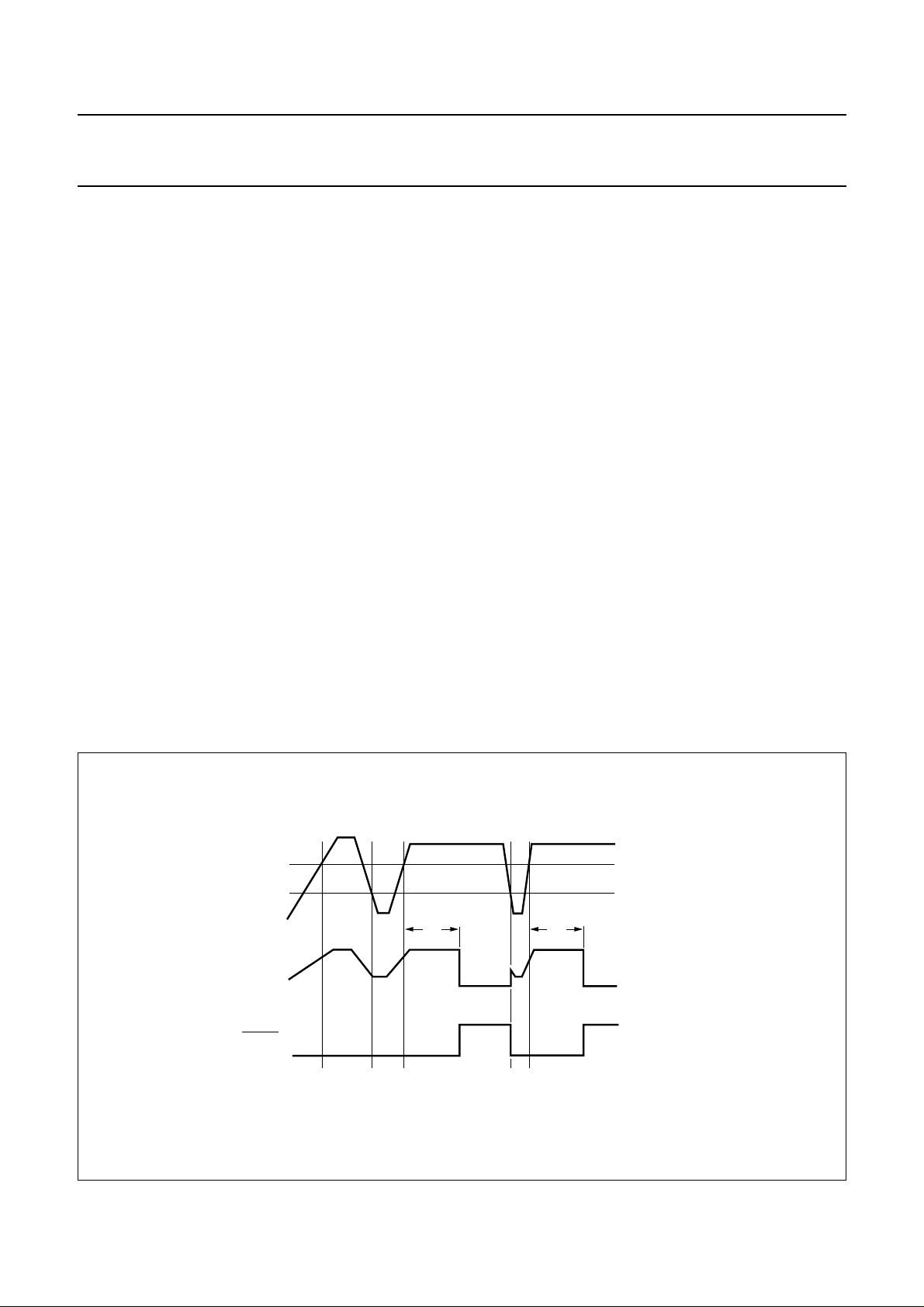
Supply voltage supervisor (V
This block surveys the V
DD
)
DD
supply. A defined reset pulse
of 10 ms minimum (tW) can be retriggered and is delivered
on the ALARM outputs during power-up or power-down of
VDD(see Fig.5). This signal is also used for eliminating the
spikes on card contacts during power-up or power-down.
When VDD reaches V
th2+Vhys2
, an internal delay is
started. The ALARM outputs are active until this delay has
expired. When VDD falls below V
, ALARM is activated
th2
and a deactivation sequence of the contacts is performed.
For 3 V supply, the supervisor option must be chosen at
3 V. For 5 V supply, both options (3 or 5 V) may be chosen
depending on the application.
Clock circuitry
The TDA8002 supports both synchronous and
2
asynchronous cards (I
C-bus memories requiring an
acknowledge signal from the master are not supported).
There are three methods to clock the circuitry:
• Apply a clock signal to pin STROBE
• Use of an internal RC oscillator
• Use of a quartz oscillator which should be connected
between pins XTAL1 and XTAL2.
When CLKSEL is HIGH, the clock should be applied on the
STROBE pin, and when CLKSEL is LOW, one of the
internal oscillators is used.
When an internal clock is used, the clock output is
available on pin CLKOUT. The RC oscillator is selected by
making CLKDIV1 HIGH and CLKDIV2 LOW. The clock
output to the card is available on pin CLK. The frequency
of the card clock can be the input frequency divided by
2 or 4, STOP LOW or 1.25 MHz, depending on the states
of CLKDIV1 or CLKDIV2 (see Table 1).
Do not change CLKSEL during activation. When in
low-power (sleep) mode, the internal oscillator frequency
which is available on pin CLKOUT is lowered to
approximately 16 kHz for power-economy purposes.
handbook, full pagewidth
V
DD
t
W
ALARM
ALARM
Fig.5 Alarm as a function of VDD (pulse width 10 ms).
1997 Nov 04 7
V
+ V
th2
hys2
V
th2
t
W
MGE734
Philips Semiconductors Product specification
IC card interface TDA8002
Table 1 Clock circuitry definition
MODE CLKSEL CLKDIV1 CLKDIV2
HIGH LOW HIGH LOW
HIGH LOW LOW LOW
HIGH LOW LOW HIGH
FREQUENCY
OF CLK
1
⁄2f
int
1
⁄4f
xtal
1
⁄2f
xtal
HIGH LOW HIGH HIGH STOP LOW f
HIGH HIGH X
LOW
(2)
(1)
X
(1)
(1)
X
(1)
X
(1)
X
STROBE f
STOP LOW
Notes
1. X = don’t care.
2. In low-power mode.
= 32 kHz in low-power mode.
3. f
int
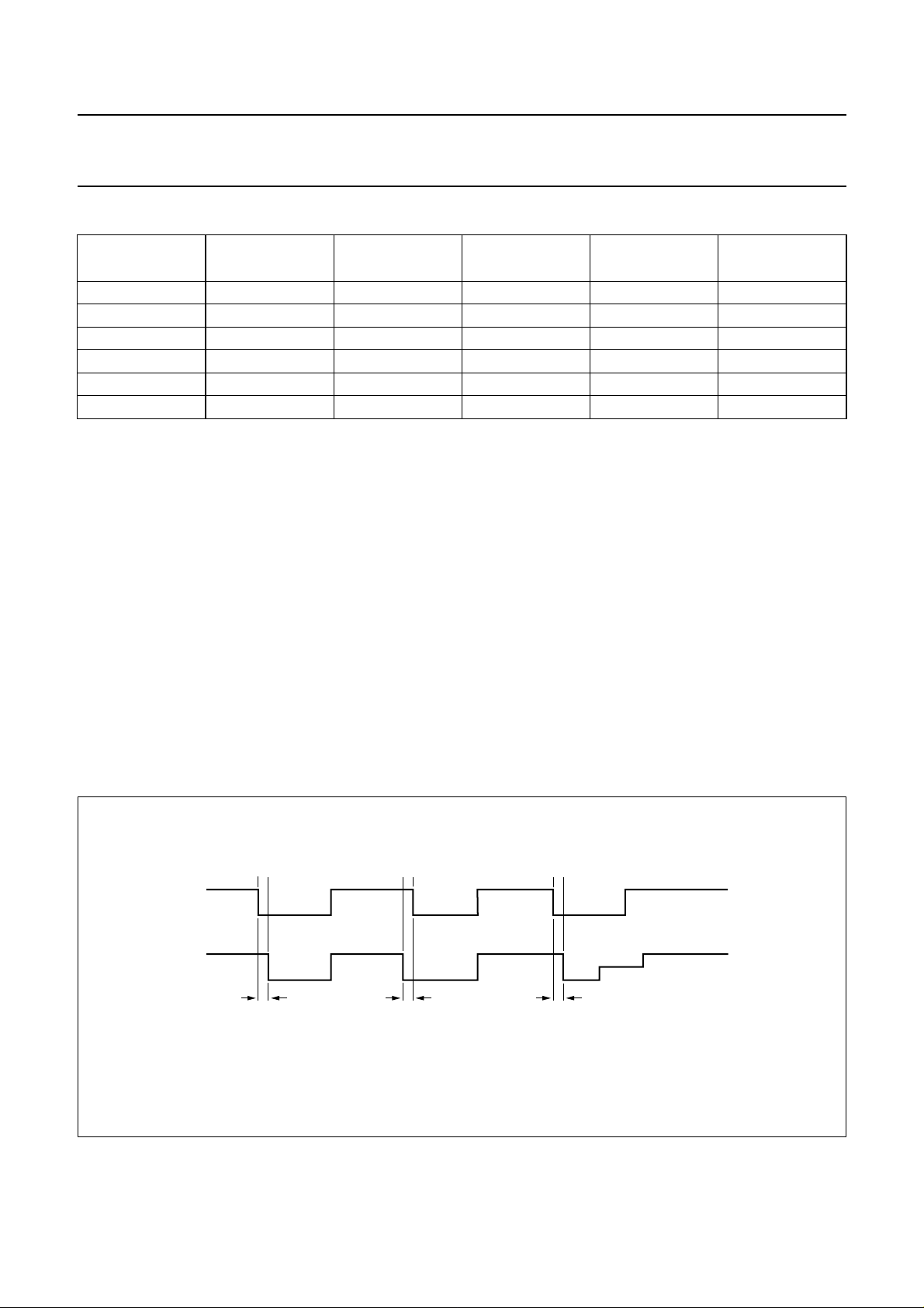
I/O circuitry
The three I/O transceivers are identical. The state is HIGH
for all I/O pins (i.e. I/O, I/OUC, AUX1, AUX1UC, AUX2 and
AUX2UC). Pin I/O is referenced to VCC and pin I/OUC to
VDD, thus ensuring proper operation in case VCC≠ VDD.
The first side on which a falling edge is detected becomes
a master (input). An anti-latch circuitry first disables the
detection of the falling edge on the other side, which
becomes slave (output).
When the input is back to HIGH level, a current booster is
turned on during the delay t
on the output side and then
d
both sides are back to their idle state, ready to detect the
next logic 0 on any side.
In case of a conflict, both lines may remain LOW until the
software enables the lines to be HIGH. The anti-latch
circuitry ensures that the lines do not remain LOW if both
sides return HIGH, regardless of the prior conditions.
The maximum frequency on the lines is approximately
1 MHz.
After a delay time td (about 50 ns), the logic 0 present on
the master side is transferred on the slave side.
FREQUENCY
OF CLKOUT
1
⁄2f
int
f
xtal
f
xtal
xtal
xtal
1
(3)
⁄2f
int
handbook, full pagewidth
I/O
I/OUC
t
d
t
d
Fig.6 Master and slave signals.
1997 Nov 04 8
t
d
conflict idle
MGD703
Philips Semiconductors Product specification
IC card interface TDA8002
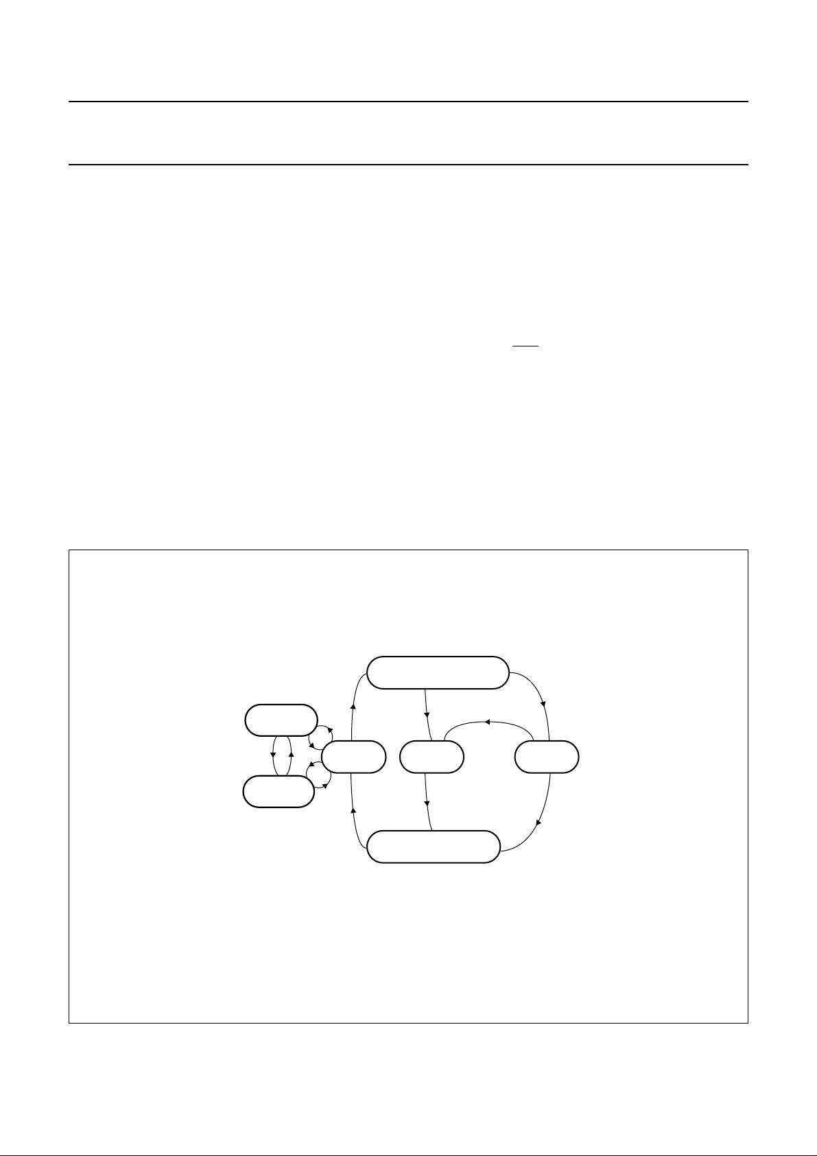
Logic circuitry
After power-up, the circuit has six possible states of
operation. Table 1 shows the sequence of these states.
I
DLE MODE
After reset, the circuit enters the idle mode.
A minimum number of functions in the circuit are active
while waiting for the microcontroller to start a session:
• All card contacts are inactive
• I/OUC, AUX1UC and AUX2UC are high-impedance
• Oscillator XTAL runs, delivering CLKOUT
• Voltage supervisor is active.
L
OW-POWER (SLEEP) MODE
When pin MODE goes LOW, the circuit enters the
low-power (sleep) mode. As long as pin MODE is LOW, no
activation is possible.
State diagram
If pin MODE goes LOW in the active mode, a normal
deactivation sequence is performed before entering
low-power mode. When pin MODE goes HIGH, the circuit
enters normal operation after a delay of at least 6 ms
(96 cycles of CLKOUT). During this time the CLKOUT
remains at 16 kHz.
• All card contacts are inactive
• Oscillator XTAL does not run
• The V
supervisor, ALARM output, card presence
DD
detection and OFF output remain functional
• Internal oscillator is slowed to 32 kHz, CLKOUT
providing 16 kHz.
A
CTIVE MODE
When the activation sequence is completed, the TDA8002
will be in the active mode. Data is exchanged between the
card and the microcontroller via the I/O lines.
handbook, full pagewidth
POWER
OFF
LOW-POWER
MODE
ACTIVATION
IDLE
MODE
FAULT
DEACTIVATION
Fig.7 State diagram.
ACTIVE
MODE
MGE735
1997 Nov 04 9
 Loading...