

Philips TDA5146T Datasheet

INTEGRATED CIRCUITS
TDA5146T
Brushless DC motor drive circuit
Product specification 1994 May 18

Philips Semiconductors Product specification
Type number
TDA5146TBrushless DC motor drive circuit
FEATURES
•Full–wave commutation (using push/pull drivers at the output stages) without position sensors
•Built–in start–up circuit
•Three push–pull outputs:
– 2 A output current (Typical)
– Built–in current limiter
•Thermal protection
•Soft switching outputs
•Flyback diodes
•Tacho output sensor
•Brake function
•Direction control input
•Reset function
•FET driver stage to be used in a buck converter
APPLICATIONS
General purpose spindle driver (e.g., HDD, tape driver)
GENERAL DESCRIPTION
The TDA5146T is a bipolar integrated circuit used to drive brushless DC motors in full–wave mode. The device senses the rotor position using
an EMF –sensing technique and is ideally suited as a drive circuit for a hard disk drive motor or tape drive.
QUICK REFERENCE DATA
Measured over full voltage and temperature ranges
Symbol
V
P
Vsup Supply for the FET driver voltage range 4 – 18 V
V
VMOT
VDo Driver output voltage drop IO= 100 mA – 0.9 1.05 V
I
LIM
NOTES:
1. An unstabilized supply can be used
2. V
VMOT=VP
; all outputs IO = 0 mA
Parameter Min. Typ. Max. Unit
Supply voltage range (Note 1) 4 – 18 V
Input voltage to the output driver stages (see Fig. 1) 1.7 – 16 V
Current limiting 1.80 2.0 2.5 A
ORDERING AND PACKAGE INFORMA TION
Package
Name Description Version
TDA5146T SO28 plastic small outline package; 28 leads; body width 7.5 mm SOT136-1
1994 May 18
2
Philips Semiconductors Product specification
TDA5146TBrushless DC motor drive circuit
VSUP PWMOUT BRAKE RESET VMOT
1994 May 18
GND2 VP GND1
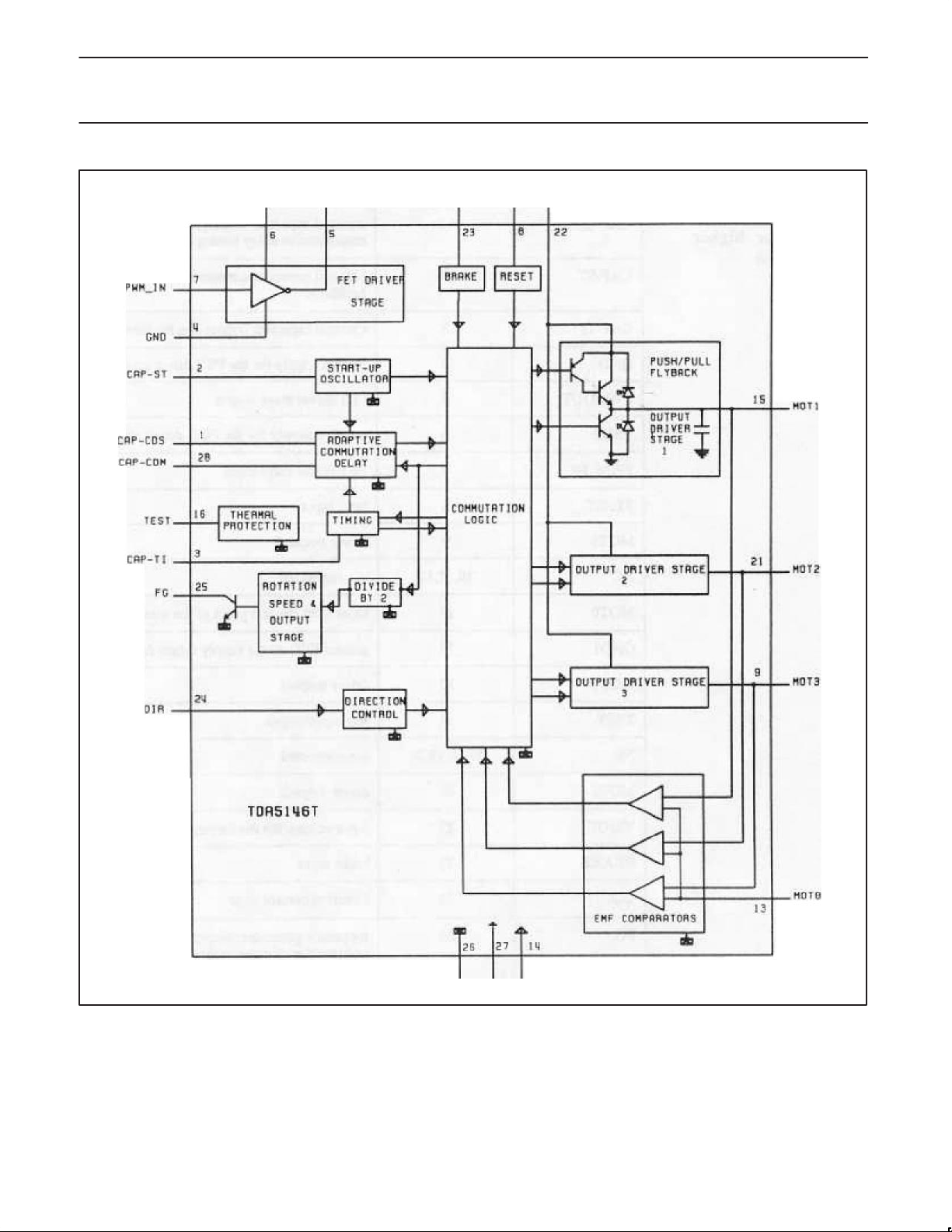
Figure 1. Block diagram
3

Philips Semiconductors Product specification
TDA5146TBrushless DC motor drive circuit
PINNING
Symbol Pin Description
CAP–CDS 1 external capacitor connection for adaptive commutation delay timing copy
CAP–ST 2 external capacitor connection for start–up oscillator
CAP–TI 3 external capacitor connection for timing
GND 4 ground supply for the FET driver stage
PWMOUT 5 FET driver stage output
V
SUP
PWM_IN 7 FET driver stage input
RESET 8 reset input
MOT3 9 driver output 3
NC 10,1 1,12 not connected
MOT0 13 input from the star point of the motor coils
GND1 14 ground (0 V) motor supply return for output stages
MOT1 15 driver output 1
TEST 16 test input/output
NC 17,18,19,20 not connected
MOT2 21 driver output 2
VMOT 22 input voltage for the output driver stages
BRAKE 23 brake input
DIR 24 direction control input
FG 25 frequency generator: output of the rotation speed and position detector stages (open collector digi-
GND2 26 ground supply return for control circuits
V
P
CAP–CDM 28 external capacitor connection for adaptive commutation delay timing
NOTE:
1. Pins 10,11,12,17,18,19 have to be connected to the ground for higher dissipation
6 positive supply for the FET driver stage
tal output, negative – going edge is valid)
27 positive supply voltage
1994 May 18
CAP–CDS
CAP–ST
PWMOUT
PWM_IN
1
2
3
CAP–TI
4
GND
5
6
V
SUP
7
8
RESET
9
MOT3
10
NC
11
NC
12 17
NC
13 16
MOT0
14 15
GND1
Figure 2. Pin configuration
4
28
27
26
25
24
23
22
21
20
19
18
CAP–CDM
V
P
GND2
FG
DIR
BRAKE
V
MOT
MOT2
NC
NC
NC
NC
TEST
MOT1
SL01520

Philips Semiconductors Product specification
TDA5146TBrushless DC motor drive circuit
FUNCTIONAL DESCRIPTION
The TDA5146T offers a sensorless three phase motor drive function. It is unique in its combination of sensorless motor drive and full–wave
drive.
The TDA5146T offers protected outputs capable of handling high currents and can be used with star or delta connected motors. It can easily be
adapted for different motors and applications. The TDA5146T offers the following features:
•Sensorless commutation by using the motor EMF
•Built–in start–up circuit
•Optimum commutation, independent of motor type or motor loading
•Built–in flyback diodes
•Three phase full–wave drive
•High output current (1.8 A)
•Outputs protected by current limiting and thermal protection of each output transistor
•Low current consumption by adaptive base–drive
•Soft switching pulse output for low radiation.
•Accurate frequency generator (FG) by using the motor BMF
•Direction of rotation controlled by one pin.
•FET driver stage to be used in a buck converter
LIMITING VALUES
In accordance with the Absolute Maximum System (IEC 134).
VP, V
V
I
V
VMOT
V
O
V
O
V
I
T
stg
T
amb
P
tot
Symbol
sup
Supply voltage – 18 V
Input voltage; all pins except VMOT (VI <18 V) –0.3 VP+0.5 V
V
input voltage –0.5 17 V
VMOT
Output voltage; PWM_OUT and PG/FG GND V
Output voltage MOT0, MOT1, MOT2 and MOT3 –1 V
Input voltage CAP–ST, CAP–TI, CAP–CD and CAP–DC – 2.5 V
Storage temperature range –55 +150 °C
Operating ambient temperature range 0 70 °C
Total power dissipation – – –
Parameter Min Max Unit
P
VMOT
+ V
V
V
D
HANDLING
Every pin withstands the ESD test according to MIL–STD–883C cross 1. Method 3015 (HBM 1500W, 100 pF 3 pulses + and 3 pulses – on each
pin referenced to ground.
1994 May 18
5

Philips Semiconductors Product specification
TDA5146TBrushless DC motor drive circuit
3.5
3.0
2.5
P
tot
2.0
(H)
1.5
1.0
0.5
0
0 10203040506070
(o)
T
amb
Figure 3. Power derating curve (SOT136-1)
SL01519
1994 May 18
6
 Loading...