

Philips TDA5145T-C3 Datasheet

DATA SH EET
Product specification
Supersedes data of March 1992
File under Integrated Circuits, IC11
June 1994
INTEGRATED CIRCUITS
Philips Semiconductors
TDA5145
Brushless DC motor drive circuit

June 1994 2
Philips Semiconductors Product specification
Brushless DC motor drive circuit TDA5145
FEATURES
• Full-wave commutation (using push/pull drivers at the
output stages) without position sensors
• Built-in start-up circuitry
• Three push-pull outputs:
– output current 2.0 A (typ.)
– built-in current limiter
– soft-switching outputs for low Electromagnetic
Interference (EMI)
• Thermal protection
• Flyback diodes
• Tacho output without extra sensor
• Motor brake facility
• Direction control input
• Reset function
• Transconductance amplifier for an external control
transistor.
APPLICATIONS
• General purpose spindle driver e.g.:
– Hard disk drive
– Tape drive
– Optical disk drive.
GENERAL DESCRIPTION
The TDA5145 is a bipolar integrated circuit used to drive
3-phase brushless DC motors in full-wave mode. The
device is sensorless (saving of 3 hall-sensors) using the
back-EMF sensing technique to sense the rotor position.
It includes bidirectional control, brake function and has a
special circuit built-in to reduce the EMI (soft switching
output stages).
QUICK REFERENCE DATA
Measured over full voltage and temperature range.
Notes
1. An unstabilized supply can be used.
2. V
VMOT
= VP; +AMP IN = −AMP IN = 0 V; all outputs IO = 0 mA.
ORDERING INFORMATION
SYMBOL PARAMETER CONDITIONS MIN. TYP. MAX. UNIT
V
P
supply voltage note 1 4 − 18 V
V
VMOT
input voltage to the output driver
stages
note 2 1.7 − 16 V
V
DO
drop-out output voltage IO= 100 mA − 0.90 1.05 V
I
LIM
current limiting V
VMOT
= 10 V; RO= 1.2 Ω 1.8 2.0 2.5 A
TYPE NUMBER
PACKAGE
PINS PIN POSITION MATERIAL CODE
TDA5145 28 DIL plastic SOT117-1
TDA5145T 28 SOL plastic SOT136-1
June 1994 3
Philips Semiconductors Product specification
Brushless DC motor drive circuit TDA5145
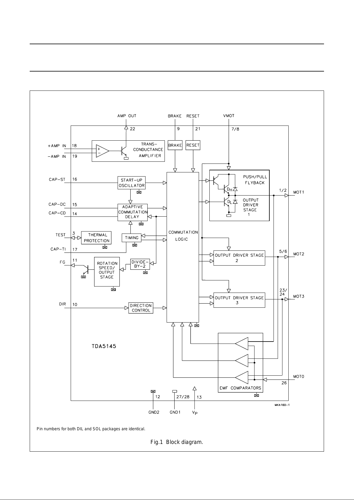
BLOCK DIAGRAM
BBBBBBBBBBBBB
B
BBBBBBBBBBBBB
B
BBBBBBBBBBBBB
B
BBBBBBBBBBBBB
B
BBBBBBBBBBBBB
B
BBBBBBBBBBBBB
B
BBBBBBBBBBBBB
B
BBBBBBBBBBBBB
B
BBBBBBBBBBBBB
B
BBBBBBBBBBBBB
B
BBBBBBBBBBBBB
B
BBBBBBBBBBBBB
B
BBBBBBBBBBBBB
B
BBBBBBBBBBBBB
B
BBBBBBBBBBBBB
B
BBBBBBBBBBBBB
B
BBBBBBBBBBBBB
B
BBBBBBBBBBBBB
B
BBBBBBBBBBBBB
B
BBBBBBBBBBBBB
B
BBBBBBBBBBBBB
B
BBBBBBBBBBBBB
B
BBBBBBBBBBBBB
B
BBBBBBBBBBBBB
B
BBBBBBBBBBBBB
B
BBBBBBBBBBBBB
B
BBBBBBBBBBBBB
B
BBBBBBBBBBBBB
B
BBBBBBBBBBBBB
B
BBBBBBBBBBBBB
B
BBBBBBBBBBBBB
B
BBBBBBBBBBBBB
B
BBBBBBBBBBBBB
B
BBBBBBBBBBBBB
B
BBBBBBBBBBBBB
B
BBBBBBBBBBBBB
B
BBBBBBBBBBBBB
B
BBBBBBBBBBBBB
B
BBBBBBBBBBBBB
B
BBBBBBBBBBBBB
B
BBBBBBBBBBBBB
B
BBBBBBBBBBBBB
B
BBBBBBBBBBBBB
B
BBBBBBBBBBBBB
B
BBBBBBBBBBBBB
B
BBBBBBBBBBBBB
B
BBBBBBBBBBBBB
B
BBBBBBBBBBBBB
B
BBBBBBBBBBBBB
B
BBBBBBBBBBBBB
B
BBBBBBBBBBBBB
B
BBBBBBBBBBBBB
B
BBBBBBBBBBBBB
B
BBBBBBBBBBBBB
B
BBBBBBBBBBBBB
B
BBBBBBBBBBBBB
B
BBBBBBBBBBBBB
B
BBBBBBBBBBBBB
B
BBBBBBBBBBBBB
B
BBBBBBBBBBBBB
B
BBBBBBBBBBBBB
B
BBBBBBBBBBBBB
B
BBBBBBBBBBBBB
B
BBBBBBBBBBBBB
B
BBBBBBBBBBBBB
B
BBBBBBBBBBBBBB
BBBBBBBBBBB
B
BBBBBBBBBBB
B
BBBBBBBBBBB
B
BBBBBBBBBBB
B
BBBBBBBBBBB
B
BBBBBBBBBBBB
BBBBBBBBBBBB
B
BBBBBBBBBBBB
B
BBBBBBBBBBBB
B
BBBBBBBBBBBB
B
BBBBBBBBBBBB
B
BBBBBBBBBBBB
B
BBBBBBBBBBBB
B
BBBBBBBBBBBBB
BBBBBBBB
B
BBBBBBBB
B
BBBBBBBB
B
BBBBBBBBB
BBBBBBBBBBBB
B
BBBBBBBBBBBB
B
BBBBBBBBBBBB
B
BBBBBBBBBBBB
B
BBBBBBBBBBBB
B
BBBBBBBBBBBBB
BBBBBBBBBBBBBBBBBBBBBBBBBBBBBBB
B
BBBBBBBBBBBBBBBBBBBBBBBBBBBBBBB
B
BBBBBBBBBBBBBBBBBBBBBBBBBBBBBBB
B
BBBBBBBBBBBBBBBBBBBBBBBBBBBBBBB
B
BBBBBBBBBBBBBBBBBBBBBBBBBBBBBBB
B
BBBBBBBBBBBBBBBBBBBBBBBBBBBBBBB
B
BBBBBBBBBBBBBBBBBBBBBBBBBBBBBBB
B
BBBBBBBBBBBBBBBBBBBBBBBBBBBBBBB
B
BBBBBBBBBBBBBBBBBBBBBBBBBBBBBBB
B
BBBBBBBBBBBBBBBBBBBBBBBBBBBBBBBB
BBBBBBBBBBBBBBBBBBBB
B
BBBBBBBBBBBBBBBBBB
B
B
BBBBBBBBBBBBBBBBBB
B
B
BBBBBBBBBBBBBBBBBB
B
B
BBBBBBBBBBBBBBBBBB
B
B
BBBBBBBBBBBBBBBBBB
B
B
BBBBBBBBBBBBBBBBBB
B
B
BBBBBBBBBBBBBBBBBB
B
B
BBBBBBBBBBBBBBBBBB
B
B
BBBBBBBBBBBBBBBBBB
B
B
BBBBBBBBBBBBBBBBBB
B
B
BBBBBBBBBBBBBBBBBB
B
B
BBBBBBBBBBBBBBBBBB
B
B
BBBBBBBBBBBBBBBBBB
B
B
BBBBBBBBBBBBBBBBBB
B
B
BBBBBBBBBBBBBBBBBB
B
B
BBBBBBBBBBBBBBBBBB
B
B
BBBBBBBBBBBBBBBBBB
B
B
BBBBBBBBBBBBBBBBBB
B
B
BBBBBBBBBBBBBBBBBB
B
B
BBBBBBBBBBBBBBBBBB
B
B
BBBBBBBBBBBBBBBBBB
B
B
BBBBBBBBBBBBBBBBBB
B
B
BBBBBBBBBBBBBBBBBB
B
B
BBBBBBBBBBBBBBBBBB
B
B
BBBBBBBBBBBBBBBBBB
B
BBBBBBBBBBBBBBBBBBBB
BBBBBBBB
B
BBBBBBBB
B
BBBBBBBB
B
BBBBBBBB
B
BBBBBBBBB
BBBBBBBBBBBBBBBBBBBBB
B
BBBBBBBBBBBBBBBBBBBBB
B
BBBBBBBBBBBBBBBBBBBBB
B
BBBBBBBBBBBBBBBBBBBBB
B
BBBBBBBBBBBBBBBBBBBBB
B
BBBBBBBBBBBBBBBBBBBBB
B
BBBBBBBBBBBBBBBBBBBBB
B
BBBBBBBBBBBBBBBBBBBBB
B
BBBBBBBBBBBBBBBBBBBBB
B
BBBBBBBBBBBBBBBBBBBBB
B
BBBBBBBBBBBBBBBBBBBBB
B
BBBBBBBBBBBBBBBBBBBBBBBBB
B
BBBBBBBBBBBBBBBBBBBBBBBBB
B
BBBBBBBBBBBBBBBBBBBBBBBBB
B
BBBBBBBBBBBBBBBBBBBBBBBBB
B
BBBBBBBBBBBBBBBBBBBBBBBBB
B
BBBBBBBBBBBBBBBBBBBBBBBBB
B
BBBBBBBBBBBBBBBBBBBBBBBBB
B
BBBBBBBBBBBBBBBBBBBBBBBBB
B
BBBBBBBBBBBBBBBBBBBBBBBBB
B
BBBBBBBBBBBBBBBBBBBBBBBBB
B
BBBBBBBBBBBBBBBBBBBBBBBBB
B
BBBBBBBBBBBBBBBBBBBBBBBBB
B
BBBBBBBBBBBBBBBBBBBBBBBBB
B
BBBBBBBBBBBBBBBBBBBBBBBBB
B
BBBBBBBBBBBBBBBBBBBBBBBBB
B
BBBBBBBBBBBBBBBBBBBBBBBBB
B
BBBBBBBBBBBBBBBBBBBBBBBBB
B
BBBBBBBBBBBBBBBBBBBBBBBBB
B
BBBBBBBBBBBBBBBBBBBBBBBBB
B
BBBBBBBBBBBBBBBBBBBBBBBBB
B
BBBBBBBBBBBBBBBBBBBBBBBBB
B
BBBBBBBBBBBBBBBBBBBBBBBBB
B
Fig.1 Block diagram.
Pin numbers for both DIL and SOL packages are identical.

June 1994 4
Philips Semiconductors Product specification
Brushless DC motor drive circuit TDA5145
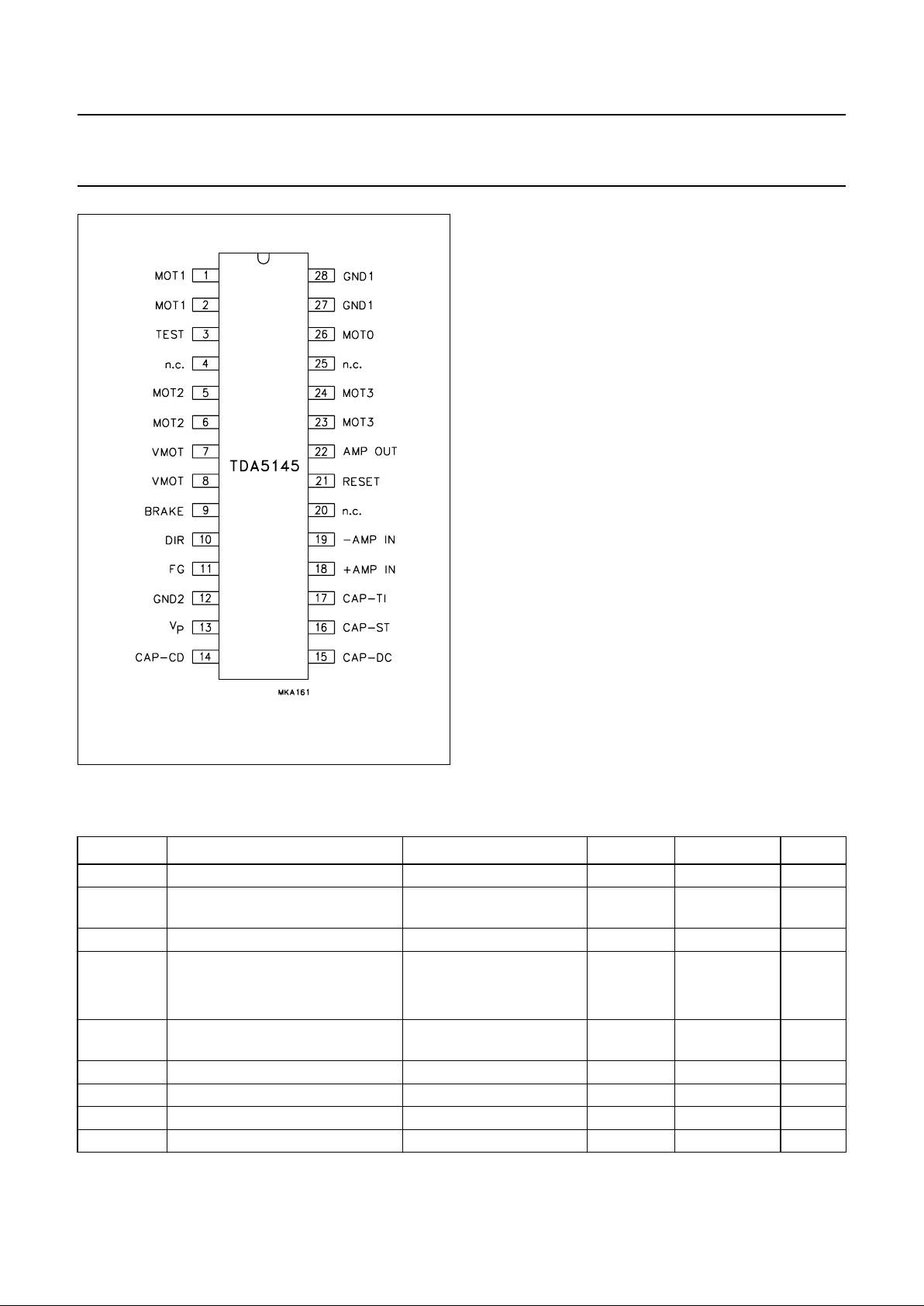
PINNING
Note
1. Pin numbers for both DIL and SOL packages are identical.
SYMBOL PIN
(1)
DESCRIPTION
MOT1 1 and 2 driver output 1
TEST 3 test input/output
n.c. 4 not connected
MOT2 5 and 6 driver output 2
VMOT 7 and 8 input voltage for the output driver stages
BRAKE 9 brake input; this pin may not be left floating, a LOW level voltage must be applied to disable
this function
DIR 10 direction control input; this pin may not be left floating
FG 11 frequency generator: output of the rotation speed (open collector digital output)
GND2 12 ground supply return for control circuits
V
P
13 supply voltage
CAP-CD 14 external capacitor connection for adaptive communication delay timing
CAP-DC 15 external capacitor connection for adaptive communication delay timing copy
CAP-ST 16 external capacitor connection for start-up oscillator
CAP-TI 17 external capacitor connection for timing
+AMP IN 18 non-inverting input of the transconductance amplifier
−AMP IN 19 inverting input of the transconductance amplifier
n.c. 20 not connected
RESET 21 reset input; this pin may not be left floating, a LOW level voltage must be applied to disable
this function
AMP OUT 22 transconductance amplifier output (open collector)
MOT3 23 and 24 driver output 3
n.c. 25 not connected
MOT0 26 input from the star point of the motor coils
GND1 27 and 28 ground (0 V) motor supply return for output stages
June 1994 5
Philips Semiconductors Product specification
Brushless DC motor drive circuit TDA5145
Fig.2 Pin configuration.
FUNCTIONAL DESCRIPTION
The TDA5145 offers a sensorless three phase motor drive
function. It is unique in its combination of sensorless motor
drive and full-wave drive. The TDA5145 offers protected
outputs capable of handling high currents and can be used
with star or delta connected motors. It can easily be
adapted for different motors and applications. The
TDA5145 offers the following features:
• Sensorless commutation by using the motor EMF.
• Built-in start-up circuit.
• Optimum commutation, independent of motor type or
motor loading.
• Built-in flyback diodes.
• Three phase full-wave drive.
• High output current (2.0 A).
• Outputs protected by current limiting and thermal
protection of each output transistor.
• Low current consumption by adaptive base-drive.
• Soft-switching pulse output for low radiation.
• Accurate frequency generator (FG) by using the
motor EMF.
• Direction of rotation controlled by one pin.
• Uncommitted operational transconductance amplifier
(OTA), with a high output current, for use as a control
amplifier.
• Brake function.
LIMITING VALUES
In accordance with the Absolute Maximum Rating System (IEC 134).
SYMBOL PARAMETER CONDITIONS MIN. MAX. UNIT
V
P
supply voltage − 18 V
V
I
input voltage; all pins except
VMOT
VI< 18 V −0.3 VP + 0.5 V
V
VMOT
VMOT input voltage −0.5 17 V
V
O
output voltage
AMP OUT and FG GND V
P
V
MOT0, MOT1, MOT2 and MOT3 −1V
VMOT
+ V
DHF
V
V
I
input voltage CAP-ST, CAP-TI,
CAP-CD and CAP-DC
− 2.5 V
T
stg
storage temperature −55 +150 °C
T
amb
operating ambient temperature 0 +70 °C
P
tot
total power dissipation see Figs 3 and 4 −− W
V
es
electrostatic handling see Chapter “Handling” − 2000 V

June 1994 6
Philips Semiconductors Product specification
Brushless DC motor drive circuit TDA5145
handbook, halfpage
50
6
4
2
0
0 200
MBD866
50 100 150
P
tot
(W)
T ( C)
amb
o
3.08
1.75
70
Fig.3 Power derating curve (SOT117-1; DIL28).
P
tot
(W)
50
3
2
0
0 200
MBD557
50 100 150
T ( C)
amb
o
1.62
1
Fig.4 Power derating curve (SOT136-1; SO28L).
HANDLING
Every pin withstands the ESD test according to
“MIL-STD-883C class 2”
. Method 3015 (HBM 1500 Ω, 100 pF) 3 pulses +
and 3 pulses − on each pin referenced to ground.
CHARACTERISTICS
V
P
= 14.5 V; T
amb
=25°C; unless otherwise specified.
SYMBOL PARAMETER CONDITIONS MIN. TYP. MAX. UNIT
Supply
V
P
supply voltage note 1 4 − 18 V
I
P
supply current note 2 − 6.8 7.8 mA
V
VMOT
input voltage to the output driver
stages
see Fig.1 1.7 − 16 V
Thermal protection
T
SD
local temperature at temperature
sensor causing shut-down
130 140 150 °C
∆T reduction in temperature before
switch-on
after shut-down − T
SD
− 30 − K

June 1994 7
Philips Semiconductors Product specification
Brushless DC motor drive circuit TDA5145
MOT0; centre tap
V
I
input voltage −0.5 − V
VMOT
V
I
I
input bias current 0.5 V < VI< V
VMOT
− 1.5 V −10 −−µA
V
CSW
comparator switching level note 3 ±20 ±25 ±30 mV
∆V
CSW
variation in comparator switching
levels
−− 3mV
V
hys
comparator input hysteresis − 75 −µV
MOT1, MOT2 and MOT3; see Fig.5
V
DO
drop-out output voltage IO= 100 mA − 0.9 1.05 V
I
O
= 1000 mA − 1.6 1.85 V
∆V
OL
variation in saturation voltage
between lower transistors
IO= 100 mA −− 180 mV
∆V
OH
variation in saturation voltage
between upper transistors
IO= −100 mA −− 180 mV
I
LIM
current limiting V
VMOT
= 10 V; RO= 1.2 Ω 1.8 2.0 2.5 A
t
r
rise time switching output V
VMOT
= 15 V; see Fig.6 5 10 15 µs
t
f
fall time switching output V
VMOT
= 15 V; see Fig.6 10 15 20 µs
V
DHF
diode forward voltage (diode DH)I
O
=−500 mA;
notes 4 and 5; see Fig.1
−− 1.5 V
V
DLF
diode forward voltage (diode DL)I
O
= 500 mA;
notes 4 and 5; see Fig.1
−1.5 −−V
I
DM
peak diode current note 5 −− 2.5 A
+AMP IN and −AMP IN
V
I
input voltage −0.3 − VP− 1.7 V
differential mode voltage without
‘latch-up’
−− ±V
P
V
I
b
input bias current −− 650 nA
C
I
input capacitance − 4 − pF
V
offset
input offset voltage −− 10 mV
AMP OUT (open collector)
I
sink
output sink current 40 −−mA
V
sat
saturation voltage II=40mA − 1.5 2.1 V
V
O
output voltage −0.5 − +18 V
SR slew rate R
L
= 330 Ω; CL=50pF − 60 − mA/µs
G
tr
transfer gain 0.3 −−S
DIR
V
IH
HIGH level input voltage 4 V < VP< 18 V 2.0 −−V
V
IL
LOW level input voltage 4 V < VP<18V −− 0.8 V
I
IL
LOW level input current −−20 −µA
I
IH
HIGH level input current − 20 −µA
SYMBOL PARAMETER CONDITIONS MIN. TYP. MAX. UNIT

June 1994 8
Philips Semiconductors Product specification
Brushless DC motor drive circuit TDA5145
RESET
V
IH
HIGH level input voltage reset mode;
4V<VP<18V
2.0 −−V
V
IL
LOW level input voltage normal mode;
4V<VP<18V
−− 0.8 V
I
IL
LOW level input current VI= 2.0 V −−20 −µA
I
IH
HIGH level input current VI= 0.8 V − 20 −µA
BRAKE
V
IH
HIGH level input voltage brake mode;
4V<VP<18V
2.0 −−V
V
IL
LOW level input voltage normal mode;
4V<VP<18V
−− 0.8 V
I
IL
LOW level input current VI= 2.0 V −−20 −µA
I
IH
HIGH level input current VI= 0.8 V − 20 −µA
FG (open collector)
V
OL
LOW level output voltage IO= 1.6 mA −− 0.4 V
V
OH(max)
maximum HIGH level output voltage V
P
−−V
t
THL
HIGH-to-LOW transition time CL= 50 pF; RL=10kΩ− 0.5 −µs
ratio of FG frequency and
commutation frequency
− 1:2 −
δ duty factor − 50 − %
CAP-ST
I
sink
output sink current 1.5 2.0 2.5 µA
I
source
output source current −2.5 −2.0 −1.5 µA
V
SWL
LOW level switching voltage − 0.20 − V
V
SWH
HIGH level switching voltage − 2.20 − V
CAP-TI
I
sink
output sink current − 28 −µA
I
source
output source current 0.2 V < V
CAP-TI
< 0.3 V −−57 −µA
0.3V<V
CAP-TI
< 2.2 V −−5−µA
V
SWL
LOW level switching voltage − 50 − mV
V
SWM
MIDDLE level switching voltage − 0.30 − V
V
SWH
HIGH level switching voltage − 2.20 − V
CAP-CD
I
sink
output sink current 10.6 16.2 22 µA
I
source
output source current −5.3 −8.1 −11 µA
I
sink/Isource
ratio of sink to source current 1.85 2.05 2.25
V
IL
LOW level input voltage 850 875 900 mV
V
IH
HIGH level input voltage 2.3 2.4 2.55 V
SYMBOL PARAMETER CONDITIONS MIN. TYP. MAX. UNIT
 Loading...