

Philips TDA5051AT, TDA5051 Datasheet

INTEGRATED CIRCUITS
DATA SH EET
TDA5051A
Home automation modem
Product specification
Supersedes data of 1997 Sep 19
File under Integrated Circuits, IC11
1999 May 31

Philips Semiconductors Product specification
Home automation modem TDA5051A
FEATURES
• Full digital carrier generation and shaping
• Modulation/demodulation frequency set by clock
adjustment, from microcontroller or on-chip oscillator
• High clock rate of 6-bit A/D (Digital to Analog) converter
for rejection of aliasing components
APPLICATIONS
• Home appliance control (air conditioning, shutters,
lighting, alarms and so on)
• Energy/heating control
• Amplitude Shift Keying (ASK) data transmission using
the home power network.
• Fully integrated output power stage with overload
protection
• Automatic Gain Control (AGC) at receiver input
• 8-bit A/D (Analog to Analog) converter and narrow
digital filtering
• Digital demodulation delivering baseband data
GENERAL DESCRIPTION
The TDA5051A is a modem IC, specifically dedicated to
ASK transmission by means of the home power supply
network, at 600 or 1200 baud data rate. It operates from a
single 5 V supply.
• Easy compliance with EN50065-1 with simple coupling
network
• Few external components for low cost applications
• SO16 plastic package.
QUICK REFERENCE DATA
SYMBOL PARAMETER CONDITIONS MIN. TYP. MAX. UNIT
V
DD
I
DD(tot)
supply voltage 4.75 5.0 5.25 V
total supply current f
= 8.48 MHz
osc
reception mode − 28 38 mA
transmission mode (
DATAIN=0) ZL=30Ω−47 68 mA
power-down mode − 19 25 mA
f
cr
f
osc
V
o(rms)
carrier frequency note 1 95 132.5 148.5 kHz
oscillator frequency 6.08 8.48 9.504 MHz
output carrier signal on CISPR16 load
120 − 122 dBµV
(RMS value)
V
i(rms)
THD total harmonic distortion on CISPR16
input signal (RMS value) note 2 82 − 122 dBµV
−−55 − dB
load with coupling network
Z
L
load impedance 1 30 −Ω
BR baud rate − 600 1200 bits/s
T
amb
ambient temperature 0 − 70 °C
Notes
1. Frequency range corresponding to the EN50065-1 band. However, the modem can operate at any lower oscillator
frequency.
2. The minimum value can be improved by using an external amplifier, see application diagrams Figs 22 and 23.
1999 May 31 2
Philips Semiconductors Product specification
Home automation modem TDA5051A
ORDERING INFORMATION
TYPE
NUMBER
NAME DESCRIPTION VERSION
PACKAGE
TDA5051AT SO16 plastic small outline package; 16 leads; body width 7.5 mm SOT162-1
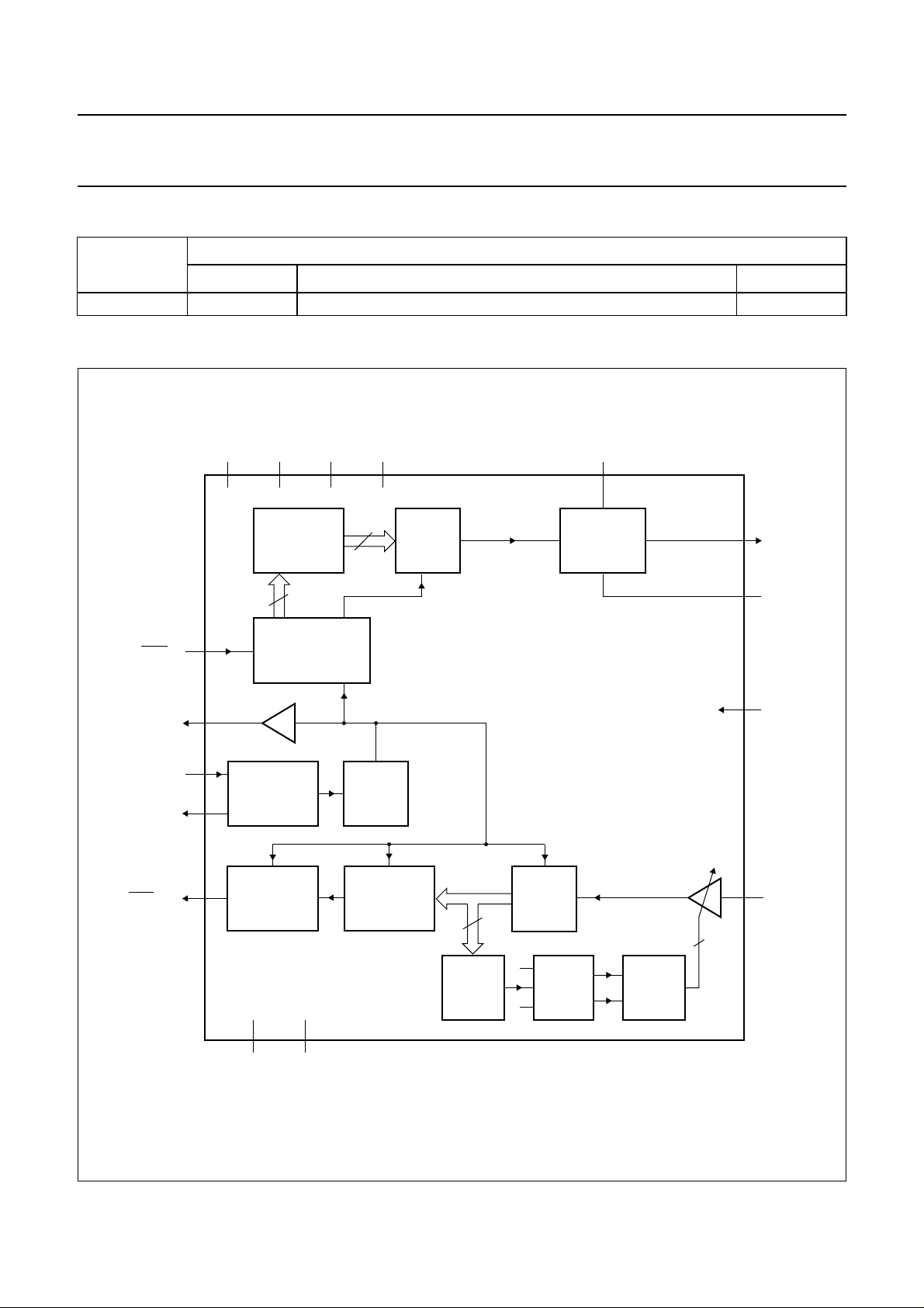
BLOCK DIAGRAM
handbook, full pagewidth
DATA
IN
CLK
OUT
DGND
1
4
AGND12V
5
CONTROL LOGIC
ROM
10
DDA
13
V
DDD
311
modulated
6
DAC clock
D/A
filter clock
carrier
V
DDAP
POWER
DRIVE
WITH
PROTECTION
TDA5051A
10
9
15
TX
OUT
APGND
PD
7
OSCILLATOR
8
2
DIGITAL
DEMODULATOR
16
TEST1 SCANTEST
2
÷
DIGITAL
BAND-PASS
FILTER
DETECT
6
DATA
OSC1
OSC2
OUT
Fig.1 Block diagram.
1999 May 31 3
PEAK
14
A/D
8
H
L
U
D
COUNT
5
U/D
MGK832
RX
IN

Philips Semiconductors Product specification
Home automation modem TDA5051A
PINNING
SYMBOL PIN DESCRIPTION
DATA
IN
DATA
OUT
V
DDD
CLK
OUT
DGND 5 digital ground
SCANTEST 6 test input (LOW in application)
OSC1 7 oscillator input
OSC2 8 oscillator output
APGND 9 analog ground for power amplifier
TX
OUT
V
DDAP
AGND 12 analog ground
V
DDA
RX
IN
PD 15 power-down input (active HIGH)
TEST1 16 test input (HIGH in application)
1 digital data input (active LOW)
2 digital data output (active LOW)
3 digital supply voltage
4 clock output
10 analog signal output
11 analog supply voltage for power
amplifier
13 analog supply voltage
14 analog signal input
handbook, halfpage
DATA
SCANTEST
DATA
CLK
OUT
V
DDD
OUT
DGND
OSC1
OSC2
IN
1
2
3
4
TDA5051AT
5
6
7
8
Fig.2 Pin configuration.
MGK833
16
15
14
13
12
11
10
9
TEST1
PD
RX
IN
V
DDA
AGND
V
DDAP
TX
OUT
APGND
FUNCTIONAL DESCRIPTION
Both transmission and reception stages are controlled
either by the master clock of the microcontroller or by the
on-chip reference oscillator connected to a crystal. This
ensures the accuracy of the transmission carrier and the
exact trimming of the digital filter, thus making the
performance totally independent of application
disturbances such as component spread, temperature,
supply drift and so on.
The interface with the power network is made by means of
an LC network (see Fig.18). The device includes a power
output stage that feeds a 120 dBµV (RMS) signal on a
typical 30 Ω load.
To reduce power consumption, the IC is disabled by a
power-down input (pin PD): in this mode, the on-chip
oscillator remains active and the clock continues to be
supplied at pin CLK
. For low-power operation in
OUT
reception mode, this pin can be dynamically controlled by
the microcontroller, see Section “Power-down mode”.
When the circuit is connected to an external clock
generator (see Fig.6), the clock signal must be applied at
pin OSC1 (pin 7); OSC2 (pin 8) must be left open-circuit.
Fig.7 shows the use of the on-chip clock circuit.
All logic inputs and outputs are compatible with
TTL/CMOS levels, providing an easy connection to a
standard microcontroller I/O port.
The digital part of the IC is fully scan-testable. Two digital
inputs, SCANTEST and TEST1, are used for production
test: these pins must be left open-circuit in functional mode
(correct levels are internally defined by pull-up or
pull-down resistors).
Transmission mode
To provide strict stability with respect to environmental
conditions, the carrier frequency is generated by scanning
the ROM memory under the control of the microcontroller
clock or the reference frequency provided by the on-chip
oscillator. High frequency clocking rejects the aliasing
components to such an extent that they are filtered by the
coupling LC network and do not cause any significant
disturbance. The data modulation is applied through
pin DATAIN and smoothly applied by specific digital circuits
to the carrier (shaping). Harmonic components are limited
in this process, thus avoiding unacceptable disturbance of
the transmission channel (according to CISPR16 and
EN50065-1 recommendations). A −55 dB Total Harmonic
Distortion (TDH) is reached when the typical LC coupling
network (or an equivalent filter) is used.
1999 May 31 4

Philips Semiconductors Product specification
Home automation modem TDA5051A
The DAC and the power stage are set in order to provide
a maximum signal level of 122 dBµV (RMS) at the output.
The output of the power stage (TX
) must always be
OUT
connected to a decoupling capacitor, because of a DC
level of 0.5VDD at this pin, which is present even when the
device is not transmitting. This pin must also be protected
against overvoltage and negative transient signals.
The DC level of TX
can be used to bias a unipolar
OUT
transient suppressor, as shown in the application diagram;
see Fig.18.
Direct connection to the mains is done through an LC
network for low-cost applications. However, a HF signal
transformer could be used when power-line insulation has
to be performed.
CAUTION
In transmission mode, the receiving part of the circuit is
not disabled and the detection of the transmitted signal
is normally performed. In this mode, the gain chosen
before the beginning of the transmission is stored, and
the AGC is internally set to −6dB as long as DATA
IN
is LOW. Then, the old gain setting is automatically
restored.
Reception mode
After digital demodulation, the baseband data signal is
made available after pulse shaping.
The signal pin (RXIN) is a high-impedance input which has
to be protected and DC decoupled for the same reasons
as with pin TX
. The high sensitivity (82 dBµV) of this
OUT
input requires an efficient 50 Hz rejection filter (realized by
the LC coupling network), which also acts as an
anti-aliasing filter for the internal digital processing;
see Fig.18.
Data format
T
RANSMISSION MODE
The data input (DATAIN) is active LOW: this means that a
burst is generated on the line (pin TX
) when DATA
OUT
IN
pin is LOW.
Pin TX
is in a high-impedance state as long as the
OUT
device is not transmitting. Successive logic 1s are treated
in a Non-Return-to-Zero (NRZ) mode, see pulse shapes in
Figs 8 and 9.
R
ECEPTION MODE
The data output (pin DATA
) is active LOW; this means
OUT
that the data output is LOW when a burst is received.
Pin DATA
remains LOW as long as a burst is received.
OUT
The input signal received by the modem is applied to a
wide range input amplifier with AGC (−6 to +30 dB). This is
basically for noise performance improvement and signal
level adjustment, which ensures a maximum sensitivity of
the ADC. An 8-bit conversion is then performed, followed
Power-down mode
Power-down input (pin PD) is active HIGH; this means that
the power consumption is minimum when pin PD is HIGH.
Now, all functions are disabled, except clock generation.
by digital band-pass filtering, to meet the CISPR
normalization and to comply with some additional
limitations met in current applications.
LIMITING VALUES
In accordance with the Absolute Maximum Rating System (IEC 134).
SYMBOL PARAMETER MIN. MAX. UNIT
V
f
T
T
T
DD
osc
stg
amb
j
supply voltage 4.5 5.5 V
oscillator frequency − 12 MHz
storage temperature −50 +150 °C
ambient temperature −10 +80 °C
junction temperature − 125 °C
HANDLING
Inputs and outputs are protected against electrostatic discharge in normal handling. However, to be totally safe, it is
desirable to take normal precautions appropriate to handling MOS devices.
1999 May 31 5

Philips Semiconductors Product specification
Home automation modem TDA5051A
CHARACTERISTICS
V
DDD=VDDA
SYMBOL PARAMETER CONDITIONS MIN. TYP. MAX. UNIT
Supply
V
DD
I
DD(RX/TX)(tot)
I
DD(PD)(tot)
I
DD(PAMP)
I
DD(PAMP)(max)
=5V±5%; T
= 0 to 70 °C; V
amb
connected to V
DDD
; DGND connected to AGND.
DDA
supply voltage 4.75 5 5.25 V
total analog + digital
supply current
total analog + digital
supply current;
VDD=5V±5%
TX or RX mode
VDD=5V±5%;
PD = HIGH
− 28 38 mA
− 19 25 mA
Power-down mode
power amplifier supply
current
VDD=5V±5%;
ZL=30Ω;
− 19 30 mA
DATAIN= LOW
in transmission mode
maximum power amplifier
supply current
VDD=5V±5%;
ZL=1Ω;
− 76 − mA
DATAIN= LOW
in transmission mode
DATAIN and PD inputs: DATA
V
IH
V
IL
V
OH
V
OL
HIGH-level input voltage 0.2VDD+ 0.9 − VDD+ 0.5 V
LOW-level input voltage −0.5 − 0.2VDD− 0.1 V
HIGH-level output voltage IOH= −1.6 mA 2.4 −− V
LOW-level output voltage IOL= 1.6 mA −−0.45 V
and CLK
OUT
OUT
outputs
OSC1 input and OSC2 output (OSC2 only used for driving external quartz crystal; must be left open-circuit
when using an external clock generator)
V
IH
V
IL
V
OH
V
OL
HIGH-level input voltage 0.7V
DD
− VDD+ 0.5 V
LOW-level input voltage −0.5 − 0.2VDD− 0.1 V
HIGH-level output voltage IOH= −1.6 mA 2.4 −− V
LOW-level output voltage IOL= 1.6 mA −−0.45 V
Clock
f
osc
f
osc
-------f
cr
f
osc
---------------------
f
CLKOUT
oscillator frequency 6.080 − 9.504 MHz
ratio between oscillator
− 64 −
and carrier frequency
ratio between oscillator
− 2 −
and clock output frequency
Transmission mode
f
cr
t
su
t
h
carrier frequency f
set-up time of the shaped
burst
hold time of the shaped
burst
= 8.48 MHz − 132.5 − kHz
osc
f
= 8.48 MHz;
osc
− 170 −µs
see Fig.8
f
= 8.48 MHz;
osc
− 170 −µs
see Fig.8
1999 May 31 6

Philips Semiconductors Product specification
Home automation modem TDA5051A
SYMBOL PARAMETER CONDITIONS MIN. TYP. MAX. UNIT
t
W(DI)(min)
V
o(rms)
I
o(max)
Z
o
V
O
THD total harmonic distortion on
B
−20dB
minimum pulse width of
DATAIN signal
output carrier signal
(RMS value)
power amplifier maximum
output current (peak value)
output impedance of the
power amplifier
output DC level at
pin TX
OUT
CISPR16 load with the
coupling network
(measured on the first ten
harmonics)
bandwidth of the shaped
output signal (at −20 dB)
on CISPR16 load with the
coupling network
f
= 8.48 MHz;
osc
see Fig.8
ZL= CISPR16;
DATAIN= LOW
ZL=1Ω;
DATAIN= LOW
V
= 121 dBµV on
o(rms)
CISPR16 load;
f
= 8.48 MHz;
osc
DATAIN= LOW
(no modulation);
see Figs 3 and 16
V
= 121 dBµV on
o(rms)
CISPR16 load;
f
= 8.48 MHz;
osc
DATAIN= 300 Hz;
duty factor = 50%;
see Fig.4
− 190 −µs
120 − 122 dBµV
− 160 − mA
− 5 −Ω
− 2.5 − V
−−55 − dB
− 3000 − Hz
Reception mode
V
i(rms)
analog input signal
(RMS value)
V
I
Z
i
R
AGC
t
c(AGC)
t
d(dem)(su)
DC level at pin RX
IN
RXIN input impedance − 50 − kΩ
AGC range − 36 − dB
AGC time constant f
demodulation delay set-up
time
t
d(dem)(h)
demodulation delay hold
time
B
det
detection bandwidth f
BER bit error rate f
82 − 122 dBµV
− 2.5 − V
= 8.48 MHz;
osc
− 296 −µs
see Fig.5
f
= 8.48 MHz;
osc
− 350 400 µs
see Fig.15
f
= 8.48 MHz;
osc
− 420 470 µs
see Fig.15
= 8.48 MHz − 3 − kHz
osc
= 8.48 MHz;
osc
− 1 − 1 × 10
600 baud; S/N = 35 dB;
signal 76 dBµV;
see Fig.17
−4
1999 May 31 7

Philips Semiconductors Product specification
Home automation modem TDA5051A
SYMBOL PARAMETER CONDITIONS MIN. TYP. MAX. UNIT
Power-up timing
t
d(pu)(TX)
delay between power-up
and DATAIN in
transmission mode
t
d(pu)(RX)
delay between power-up
and DATA
mode
Power-down timing
t
d(pd)(TX)
delay between PD = 0 and
DA TAIN in transmission
mode
t
d(pd)(RX)
delay between PD = 0 and
DA TA
mode
t
active(min)
minimum active time with
T = 10 ms power-down
period in reception mode
OUT
in reception
OUT
in reception
XTAL = 8.48 MHz;
C1 = C2 = 27 pF;
Rp= 2.2 MΩ; see Fig.10
XTAL = 8.48 MHz;
C1 = C2 = 27 pF;
Rp= 2.2 MΩ;
f
= 132.5 kHz;
RXIN
120 dBµV sine wave;
see Fig.11
f
= 8.48 MHz;
osc
see Fig.12
f
= 8.48 MHz;
osc
f
= 132.5 kHz;
RXIN
120 dBµV sine wave;
see Fig.13
f
= 8.48 MHz;
osc
f
= 132.5 kHz;
RXIN
120 dBµV sine wave;
see Fig.14
− 1 −µs
− 1 −µs
− 10 −µs
− 500 −µs
− 1 −µs
book, full pagewidth
0
V
o(rms)
(dBV)
−100
5
10
Resolution bandwidth =9 kHz; top: 0 dBV (RMS) = 120 dBµV (RMS); marker at −5 dBV (RMS) = 115 dBµV (RMS);
the CISPR16 network provides an attenuation of 6 dB, so the signal amplitude is 121 dBµV (RMS).
132.5 kHz
Fig.3 Carrier spectrum.
f (Hz)
MGK834
6
10
1999 May 31 8

Philips Semiconductors Product specification
Home automation modem TDA5051A
handbook, full pagewidth
−10
dBV
(RMS)
−60
117.5 132.5
Resolution bandwidth = 100 Hz; B
= 3000 Hz (2 × 1500 Hz).
−20dB
1500 Hz
20 dB
Fig.4 Shaped signal spectrum.
f (kHz)
MBH664
147.5
handbook, full pagewidth
V
RXIN
V
G
AGC
+30 dB
−6 dB
(I)
0
(AGC time constant)
modulated sine wave 122 dBµV amplitude
t
c(AGC)
Fig.5 AGC time constant definition (not to scale).
1999 May 31 9
t
8.68 dB
AGC range
MGK011
 Loading...