

INTEGRATED CIRCUITS
DATA SH EET
TDA4672
Picture Signal Improvement (PSI)
circuit with enhanced peaking
function
Product specification
Supersedes data of August 1993
File under Integrated Circuits, IC02
1996 Dec 11
Philips Semiconductors Product specification
Picture Signal Improvement (PSI) circuit
with enhanced peaking function
FEATURES
• Luminance signal delay from 20 ns to 1100 ns
(minimum step 45 ns)
• Selectable luminance signal peaking with symmetrical
overshoots
• Selectable 2.6 or 5 MHz peaking centre frequency and
degree of peaking from −6 dB to +9 dB in 16 steps of
1 dB each
• Selectable noise reduction by coring
• Selectable 5 or 12 V sandcastle input voltage
2
• All controls selected via the I
• Timing pulse generation for clamping and delay time
control synchronized by sandcastle pulse
• Automatic luminance signal delay correction using a
control loop
• Luminance input signal clamping with coupling capacitor
• 4.5 to +8.8 V supply voltage
• Minimum of external components.
C-bus
TDA4672
GENERAL DESCRIPTION
The TDA4672 delays the luminance signal. The luminance
signal can also be improved by peaking and noise
reduction (coring).
QUICK REFERENCE DATA
SYMBOL PARAMETER MIN. TYP. MAX. UNIT
V
P
I
P(tot)
t
d(Y)
V
i(Y)(p-p)
G
Y
T
amb
supply voltage (pin 1) 4.5 5 8.8 V
total supply current 26 37 46 mA
Y signal delay time 20 − 1130 ns
composite Y input signal (peak-to-peak value, pin 16) − 450 640 mV
voltage gain of Y channel −−1−dB
operating ambient temperature 0 − 70 °C
ORDERING INFORMATION
TYPE
NUMBER
NAME DESCRIPTION VERSION
PACKAGE
TDA4672 DIP18 plastic dual in-line package; 18 leads (300 mil) SOT102-1
1996 Dec 11 2
Philips Semiconductors Product specification
Picture Signal Improvement (PSI) circuit
with enhanced peaking function
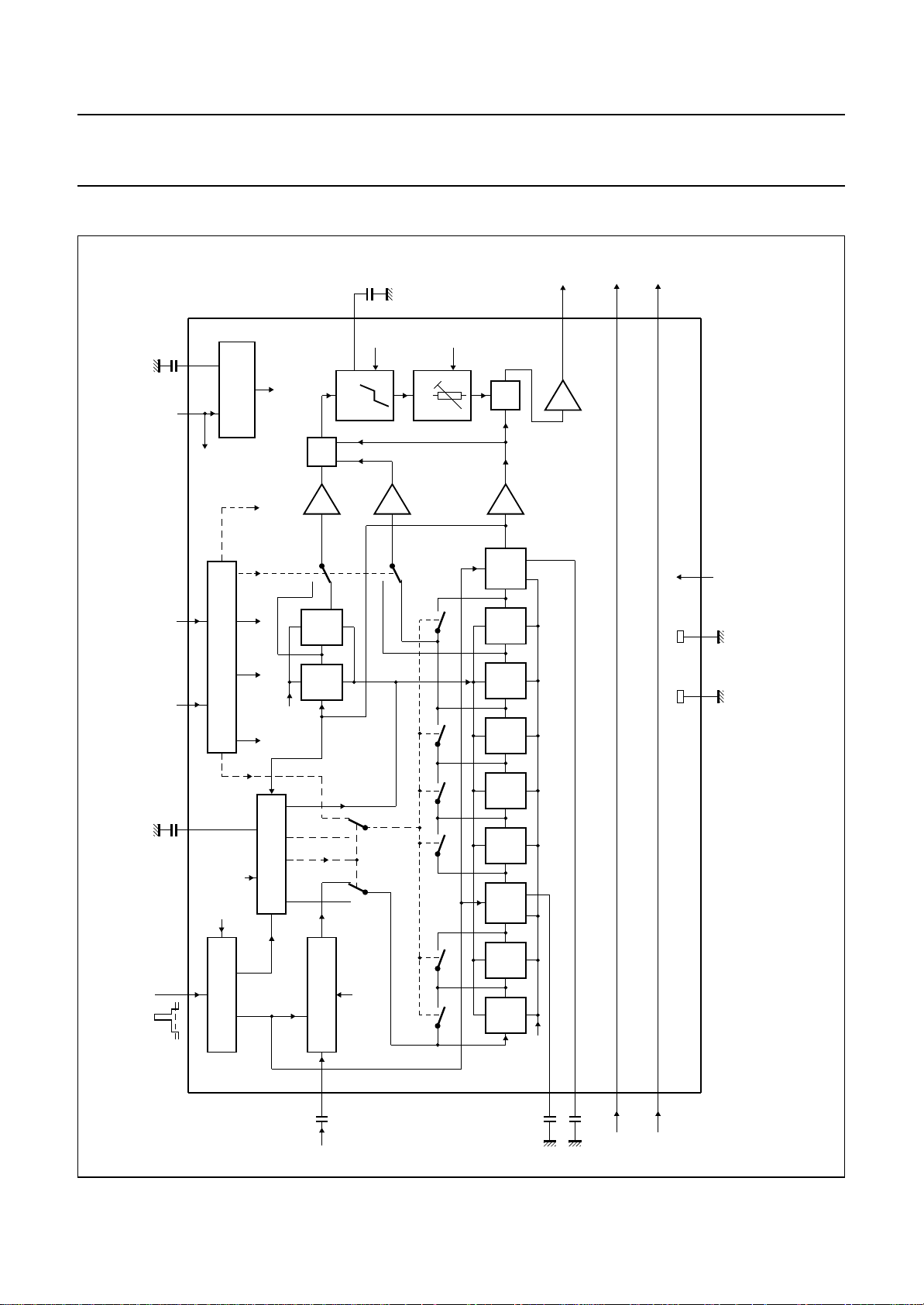
BLOCK DIAGRAM
nF
100
11
100 nF
15
1
= 5 to 8 V
P
V
ref
V
GENERATION
degree of
peaking
peaking
frequency
ref
V
CORING
+
−0.5
5 MHz
CORING
2.6 MHz
−0.5
5 MHz
C-BUS
2
I
2.6 MHz
PEAKING
C-BUS
2
I
BLACK
+
+1
LEVEL
CLAMP
Y
12
TDA4672
TDA4672
−(B − Y)
−(R − Y)
6
4
MED756
n.c.
SCL
9 10
SDA
100 nF
2
sandcastle
pulse
17
coring
on/off
CTI
on/off
C-BUS RECEIVER
2
I
REF
5 V/12 V
sandcastle
V
Y delay
ref
CONTROL
V
DELAY TIME
C-BUS
2
I
BK, H + V
BK
DETECTOR
SANDCASTLE PULSE
ns
90
ns
100
ref
V
CLAMP
BLACK LEVEL
16
control signal
ns
100
ns
90
ns
45
ns
90
ns
180
LEVEL
BLACK
ns
180
ns
450
CLAMP
V
handbook, full pagewidth
8 18 5
Fig.1 Block diagram.
ref
3
14
7
1996 Dec 11 3
100 nF
Y
100 nF13100 nF
−(R − Y)
−(B − Y)
Philips Semiconductors Product specification
Picture Signal Improvement (PSI) circuit
with enhanced peaking function
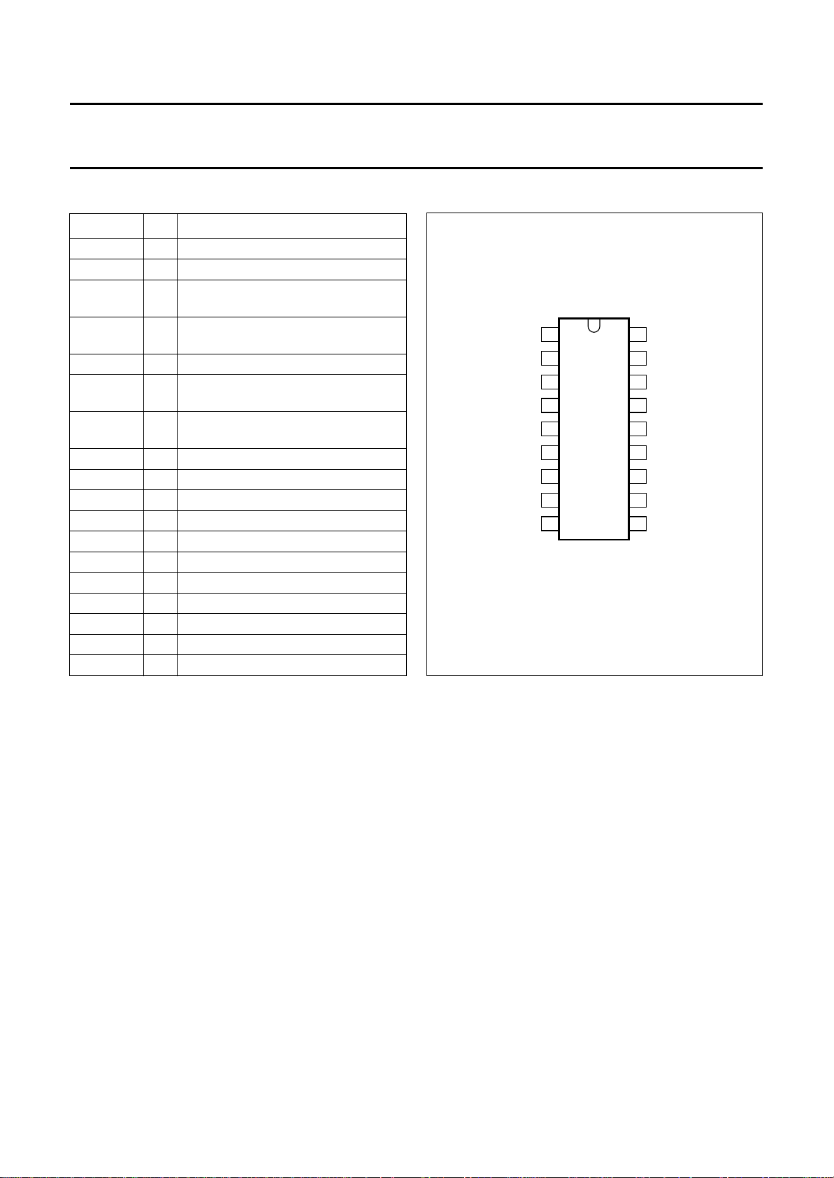
PINNING
SYMBOL PIN DESCRIPTION
V
P
C
DL
V
i(R − Y)
V
o(R − Y)
n.c. 5 not connected
V
o(B − Y)
V
i(B − Y)
GND2 8 ground 2 (0 V)
SDA 9 I
SCL 10 I
C
COR
V
oY
C
CLP1
C
CLP2
C
ref
V
iY
SAND 17 sandcastle pulse input
GND1 18 ground 1 (0 V)
1 positive supply voltage
2 capacitor of delay time control
±(R − Y) colour-difference input
3
signal; note 1
±(R − Y) colour-difference output
4
signal; note 1
±(B − Y) colour-difference output
6
signal; note 2
±(B − Y) colour-difference input
7
signal; note 2
2
C-bus serial data input/output
2
C-bus serial clock input
11 coring capacitor
12 delayed luminance output signal
13 black level clamping capacitor 1
14 black level clamping capacitor 2
15 capacitor of reference voltage
16 luminance input signal
handbook, halfpage
V
1
P
C
2
DL
V
i(R − Y)
V
o(R − Y)
V
o(B − Y)
V
i(B − Y)
n.c.
GND2
SDA
3
4
5
6
7
8
9
TDA4672
Fig.2 Pin configuration.
MED757
TDA4672
GND1
18
SAND
17
V
16
iY
C
15
ref
C
14
CLP2
C
13
CLP1
V
12
oY
C
11
COR
SCL
10
Notes
1. Pin 3 is connected directly to pin 4.
2. Pin 7 is connected directly to pin 6.
1996 Dec 11 4

Philips Semiconductors Product specification
Picture Signal Improvement (PSI) circuit
with enhanced peaking function
FUNCTIONAL DESCRIPTION
The TDA4672 contains luminance signal processing.
The luminance signal section comprises a variable,
integrated luminance delay line with luminance signal
peaking and noise reduction by coring.
All functions and parameters are controlled via the
I2C-bus.
Y-signal path
The video and blanking signal is AC-coupled to the input
pin 16. Its black porch is clamped to a DC reference
voltage to ensure the correct operating range of the
luminance delay stage.
The luminance delay line consists of all-pass filter sections
with delay times of 45, 90, 100, 180 and 450 ns
(see Fig.1). The luminance signal delay is controlled via
2
the I
C-bus in steps of 45 ns in the range of 20 to 1100 ns,
this ensures that the maximum delay difference between
the luminance and colour-difference signals is ±22.5 ns.
An automatic luminance delay time adjustment in an
internal control loop (with the horizontal frequency as a
reference) is used to correct changes in the delay time,
due to component tolerances. The control loop is
automatically enabled between the burst key pulses of
lines 16 (330) and 17 (331) during the vertical blanking
interval. The control voltage is stored in the capacitor C
connected to pin 2.
DL
TDA4672
The peaking section uses a transversal filter circuit with
selectable centre frequencies of 2.6 and 5.0 MHz.
It provides selectable degrees of peaking from−6to+9dB
and noise reduction by coring, which attenuates the
high-frequency noise introduced by peaking.
The output buffer stage ensures a low-ohmic Video
Blanking Synchronization (VBS) output signal on pin 12
(<160 Ω). The gain of the luminance signal path from
pin 16 to pin 12 is unity.
An oscillation signal of the delay time control loop is
present on output pin 12 instead of the VBS signal. It is
present during the vertical blanking interval of the burst key
pulses in lines 16 (330) to 18 (332). This sync should not
be applied for synchronization.
Colour-difference signal paths
The colour-difference input signals (on pins 3 and 7) are
connected directly to the output pins.
This is for compatibility with other Philips Semiconductors
PSI-circuits.
1996 Dec 11 5
 Loading...