

Philips TDA4662T-V3, TDA4662T-V1, TDA4662T-V2, TDA4662-V3, TDA4662-V2 Datasheet
DATA SH EET
Product specification
Supersedes data of 1995 Oct 30
File under Integrated Circuits, IC02
1996 Nov 14
INTEGRATED CIRCUITS
TDA4662
Baseband delay line
1996 Nov 14 2
Philips Semiconductors Product specification
Baseband delay line TDA4662
FEATURES
• Two comb filters, using the switched-capacitor
technique, for one line delay time (64 µs)
• For PAL and NTSC
• Adjustment-free application
• Handles negative or positive colour-difference input
signals
• Clamping of AC-coupled input signals [±(R−Y) and
±(B−Y)]
• VCO without external components
• 3 MHz internal clock signal derived from a 6 MHz CCO,
line-locked by the sandcastle pulse (64 µs line)
• Sample-and-hold circuits and low-pass filters to
suppress the 3 MHz clock signal
• Addition of delayed and non-delayed output signals
• Output buffer amplifiers
• Comb filtering functions for NTSC colour-difference
signals to suppress cross-colour.
GENERAL DESCRIPTION
The TDA4662 is an integrated baseband delay line circuit
with one line delay. It is suitable for PAL and NTSC
decoders with colour-difference signal outputs±(R−Y) and
±(B−Y).
QUICK REFERENCE DATA
ORDERING INFORMATION
SYMBOL PARAMETER MIN. TYP. MAX. UNIT
V
P1
analog supply voltage (pin 9) 4.5 5 6 V
V
P2
digital supply voltage (pin 1) 4.5 5 6 V
I
P(tot)
total supply current − 5.5 7.0 mA
V
i(p-p)
±(R−Y) input signal PAL/NTSC (peak-to-peak value; pin 16) − 525 − mV
±(B−Y) input signal PAL/NTSC (peak-to-peak value; pin 14) − 665 − mV
G
v
voltage gain VO/VI of colour-difference output signals
V
11/V16
for PAL and NTSC 5.3 5.8 6.3 dB
V
12/V14
for PAL and NTSC 5.3 5.8 6.3 dB
TYPE
NUMBER
PACKAGE
NAME DESCRIPTION VERSION
TDA4662 DIP16 plastic dual in-line package; 16 leads (300 mil) SOT38-4
TDA4662T SO16 plastic small outline package; 16 leads; body width 3.9 mm SOT109-1
1996 Nov 14 3
Philips Semiconductors Product specification
Baseband delay line TDA4662
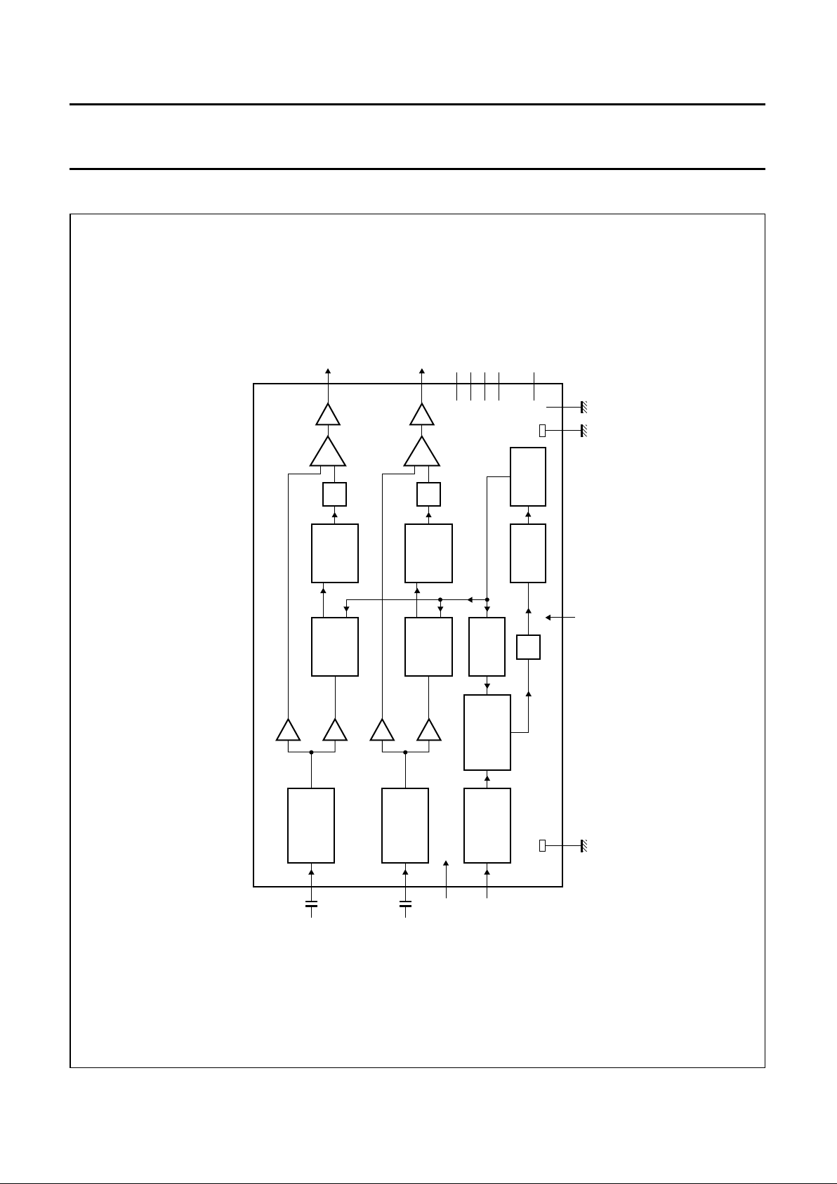
BLOCK DIAGRAM
Fig.1 Block diagram.
handbook, full pagewidth
SANDCASTLE
DETECTOR
FREQUENCY
PHASE
DETECTOR
DIVIDE-
BY-192
LP
V
P2
3 MHz shifting clock
1
digital supply
LINE
MEMORY
SIGNAL
CLAMPING
SAMPLE-
AND-HOLD
6 MHz
CCO
DIVIDE-
BY-2
LP
addition
stages
output
buffers
colour-difference
output signals
colour-difference
input signals
12
2
5
10
GND1
3
n.c.
6
n.c.13n.c.15n.c.7i.c.
4, 8
±(B−Y)
±(R−Y)
±(R−Y)
±(B−Y)
V
P1
sandcastle
input
GND2
9
14
LINE
MEMORY
TDA4662
SIGNAL
CLAMPING
pre-amplifiers
SAMPLE-
AND-HOLD
LP
11
16
analog supply
MED743
1996 Nov 14 4
Philips Semiconductors Product specification
Baseband delay line TDA4662
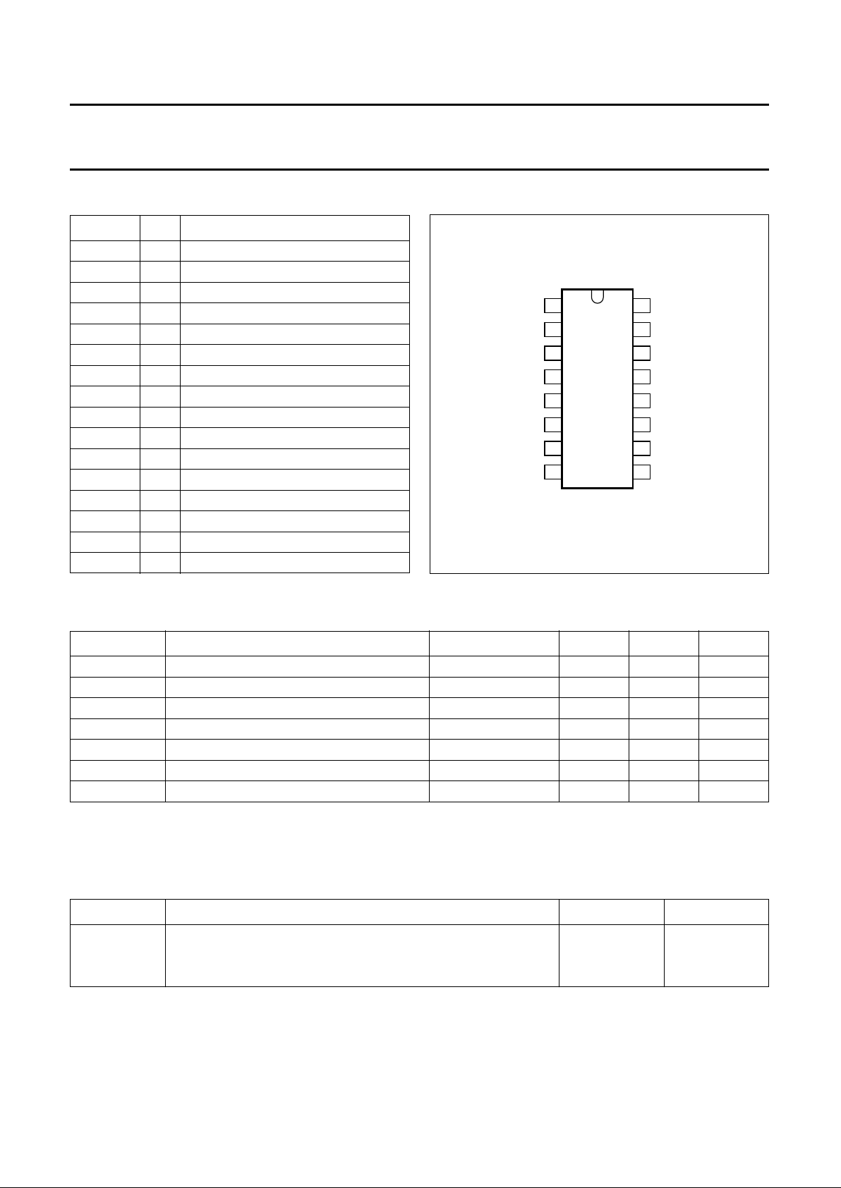
PINNING
SYMBOL PIN DESCRIPTION
V
P2
1 supply voltage for digital part (+5 V)
n.c. 2 not connected
GND2 3 ground for digital part (0 V)
i.c. 4 internally connected
SAND 5 sandcastle pulse input
n.c. 6 not connected
i.c. 7 internally connected
i.c. 8 internally connected
V
P1
9 supply voltage for analog part (+5 V)
GND1 10 ground for analog part (0 V)
V
o(R−Y)
11 ±(R−Y) output signal
V
o(B−Y)
12 ±(B−Y) output signal
n.c. 13 not connected
V
i(B−Y)
14 ±(B−Y) input signal
n.c. 15 not connected
V
i(R−Y)
16 ±(R−Y) input signal
Fig.2 Pin configuration.
handbook, halfpage
TDA4662
MED744
1
2
3
4
5
6
7
8
16
15
14
13
12
11
10
9
V
P2
n.c.
GND2
i.c.
SAND
n.c.
i.c.
i.c.
V
P1
GND1
V
o(R−Y)
V
o(B−Y)
n.c.
V
i(B−Y)
n.c.
V
i(R−Y)
LIMITING VALUES
In accordance with the Absolute Maximum Rating System (IEC 134). Ground pins 3 and 10 connected together.
Note
1. Equivalent to discharging a 200 pF capacitor through a 0 Ω series resistor.
THERMAL CHARACTERISTICS
SYMBOL PARAMETER CONDITIONS MIN. MAX. UNIT
V
P1
supply voltage (pin 9) −0.5 +7 V
V
P2
supply voltage (pin 1) −0.5 +7 V
V
5
input voltage on pin 5 −0.5 VP+ 1.0 V
V
n
voltage on pins 11, 12, 14 and 16 −0.5 V
P
V
T
stg
storage temperature −25 +150 °C
T
amb
operating ambient temperature 0 70 °C
V
ESD
electrostatic handling for all pins note 1 −±500 V
SYMBOL PARAMETER VALUE UNIT
R
th j-a
thermal resistance from junction to ambient in free air
SOT38-4 75 K/W
SOT109-1 220 K/W
 Loading...